SNAS468D September 2008 – December 2014 ADC161S626
PRODUCTION DATA.
- 1 Features
- 2 Applications
- 3 Description
- 4 Revision History
- 5 Pin Configuration and Functions
- 6 Specifications
- 7 Detailed Description
- 8 Application and Implementation
- 9 Power Supply Recommendations
- 10Layout
- 11Device and Documentation Support
- 12Mechanical, Packaging, and Orderable Information
Package Options
Mechanical Data (Package|Pins)
- DGS|10
Thermal pad, mechanical data (Package|Pins)
Orderable Information
6 Specifications
6.1 Absolute Maximum Ratings(1)(3)(2)
| MIN | MAX | UNIT | ||
|---|---|---|---|---|
| Analog Supply Voltage VA | −0.3 | 6.5 | V | |
| Digital I/O Supply Voltage VIO | −0.3 | 6.5 | V | |
| Voltage on Any Analog Input Pin to GND | −0.3 | (VA + 0.3) | V | |
| Voltage on Any Digital Input Pin to GND | −0.3 | (VIO + 0.3) | V | |
| Input Current at Any Pin(4) | –10 | 10 | mA | |
| Package Input Current(4) | –50 | 50 | mA | |
| Power Consumption at TA = 25°C | See (5) | |||
| Junction Temperature | 150 | °C | ||
| Storage temperature, Tstg | −65 | 150 | °C | |
(1) Stresses beyond those listed under Absolute Maximum Ratings may cause permanent damage to the device. These are stress ratings only, which do not imply functional operation of the device at these or any other conditions beyond those indicated under Recommended Operating Conditions. Exposure to absolute-maximum-rated conditions for extended periods may affect device reliability.
(2) If Military/Aerospace specified devices are required, please contact the TI Sales Office/ Distributors for availability and specifications.
(3) All voltages are measured with respect to GND = 0 V, unless otherwise specified.
(4) When the input voltage at any pin exceeds the power supplies (that is, VIN < GND or VIN > VA), the current at that pin should be limited to 10 mA. The 50 mA maximum package input current rating limits the number of pins that can safely exceed the power supplies with an input current of 10 mA to five.
(5) The absolute maximum junction temperature (TJmax) for this device is 150°C. The maximum allowable power dissipation is dictated by TJmax, the junction-to-ambient thermal resistance (θJA), and the ambient temperature (TA), and can be calculated using the formula PDMAX = (TJmax − TA)/θJA. The values for maximum power dissipation listed above will be reached only when the ADC161S626 is operated in a severe fault condition (e.g. when input or output pins are driven beyond the power supply voltages, or the power supply polarity is reversed). Such conditions should always be avoided.
6.2 ESD Ratings
| VALUE | UNIT | |||
|---|---|---|---|---|
| V(ESD) | Electrostatic discharge | Human body model (HBM), per ANSI/ESDA/JEDEC JS-001(1) | ±2500 | V |
| Charged-device model (CDM), per JEDEC specification JESD22-C101(2) | ±1250 | |||
| Machine model (MM) | 250 | |||
(1) JEDEC document JEP155 states that 500-V HBM allows safe manufacturing with a standard ESD control process.
(2) JEDEC document JEP157 states that 250-V CDM allows safe manufacturing with a standard ESD control process.
6.3 Recommended Operating Conditions
over operating free-air temperature range (unless otherwise noted)(1)| MIN | MAX | UNIT | |
|---|---|---|---|
| Operating Temperature Range | −40 | 85 | °C |
| Supply Voltage, VA | 4.5 | 5.5 | V |
| Supply Voltage, VIO | 2.7 | 5.5 | V |
| Reference Voltage, VREF | 0.5 | VA | V |
| Analog Input Pins Voltage Range | 0 | VA | V |
| Differential Analog Input Voltage | −VREF | +VREF | V |
| Input Common-Mode Voltage, VCM | See Figure 44 | ||
| Digital Input Pins Voltage Range | 0 | VIO | V |
| Clock Frequency | 1 | 5 | MHz |
(1) All voltages are measured with respect to GND = 0V, unless otherwise specified.
6.4 Thermal Information
| THERMAL METRIC(1) | ADC161S626 | UNIT | |
|---|---|---|---|
| DGS | |||
| 10 PINS | |||
| RθJA | Junction-to-ambient thermal resistance | 163 | °C/W |
| RθJC(top) | Junction-to-case (top) thermal resistance | 57 | |
| RθJB | Junction-to-board thermal resistance | 82 | |
| ψJT | Junction-to-top characterization parameter | 6 | |
| ψJB | Junction-to-board characterization parameter | 81 | |
(1) For more information about traditional and new thermal metrics, see the IC Package Thermal Metrics application report, SPRA953.
6.5 Converter Electrical Characteristics
The following specifications apply for VA = 4.5 V to 5.5 V, VIO = 2.7 V to 5.5 V, and VREF = 2.5 V to 5.5 V for fSCLK = 1 MHz to 4 MHz or VREF = 4.5 V to 5.5 V for fSCLK = 1 MHz to 5 MHz; fIN = 20 kHz, and CL = 25 pF, unless otherwise noted. Maximum and minimum values apply for TA = TMIN to TMAX; the typical values are tested at TA = 25°C.(1)| PARAMETER | TEST CONDITIONS | MIN | TYP | MAX | UNIT | ||
|---|---|---|---|---|---|---|---|
| STATIC CONVERTER CHARACTERISTICS | |||||||
| Resolution with No Missing Codes | 16 | Bits | |||||
| DNL | Differential Non-Linearity | −1 | -0.5/+0.8 | +2 | LSB | ||
| INL | Integral Non-Linearity | −2 | ±0.8 | +2 | LSB | ||
| OE | Offset Error | VREF = 2.5 V | −1 | −0.1 | +1 | mV | |
| VREF = 5 V | −0.4 | mV | |||||
| OEDRIFT | Offset Error Temperature Drift | VREF = 2.5 V | 3.7 | µV/°C | |||
| VREF = 5 V | 2.5 | µV/°C | |||||
| FSE | Positive Full-Scale Error | –0.03 | −0.003 | 0.03 | %FS | ||
| Negative Full-Scale Error | –0.03 | −0.002 | 0.03 | %FS | |||
| GE | Positive Gain Error | –0.02 | −0.002 | 0.02 | %FS | ||
| Negative Gain Error | –0.02 | −0.0001 | 0.02 | %FS | |||
| GEDRIFT | Gain Error Temperature Drift | 0.3 | ppm/°C | ||||
| DYNAMIC CONVERTER CHARACTERISTICS | |||||||
| SINAD | Signal-to-Noise Plus Distortion Ratio | VREF = 2.5 V | 85 | 88 | dBc | ||
| VREF = 4.5 V to 5.5 V | 89 | 93.0 | dBc | ||||
| SNR | Signal-to-Noise Ratio | VREF = 2.5 V | 85 | 88 | dBc | ||
| VREF = 4.5 V to 5.5 V | 89 | 93.2 | dBc | ||||
| THD | Total Harmonic Distortion | VREF = 2.5 V | −104 | dBc | |||
| VREF = 4.5 V to 5.5 V | −106 | dBc | |||||
| SFDR | Spurious-Free Dynamic Range | VREF = 2.5 V | 108 | dBc | |||
| VREF = 4.5 V to 5.5 V | 111 | dBc | |||||
| ENOB | Effective Number of Bits | VREF = 2.5 V | 13.8 | 14.3 | bits | ||
| VREF = 4.5 V to 5.5 V | 14.5 | 15.2 | bits | ||||
| FPBW | −3 dB Full Power Bandwidth | Output at 70.7%FS with FS Differential Input | 26 | MHz | |||
| ANALOG INPUT CHARACTERISTICS | |||||||
| VIN | Differential Input Range | −VREF | +VREF | V | |||
| IINA | Analog Input Current | CS high | –1 | 1 | µA | ||
| VREF = 5 V, VIN = 0 V, fS = 50 kSPS | 3.2 | nA | |||||
| VREF = 5 V, VIN = 0 V, fS = 200 kSPS | 10.3 | nA | |||||
| CINA | Input Capacitance (+IN or −IN) | In Acquisition Mode | 20 | pF | |||
| In Conversion Mode | 4 | pF | |||||
| CMRR | Common Mode Rejection Ratio | See the Specification Definitions for the test condition | 85 | dB | |||
| DIGITAL INPUT CHARACTERISTICS | |||||||
| VIH | Input High Voltage | fIN = 0 Hz | 0.7 x VIO | 1.9 | V | ||
| VIL | Input Low Voltage | fIN = 0 Hz | 1.7 | 0.3 x VIO | V | ||
| IIND | Digital Input Current | –1 | 1 | µA | |||
| CIND | Input Capacitance | 4 | pF | ||||
| DIGITAL OUTPUT CHARACTERISTICS | |||||||
| VOH | Output High Voltage | ISOURCE = 200 µA | VIO − 0.2 | VIO − 0.03 | V | ||
| ISOURCE = 1 mA | VIO − 0.09 | V | |||||
| VOL | Output Low Voltage | ISOURCE = 200 µA | 0.01 | 0.4 | V | ||
| ISOURCE = 1 mA | 0.07 | V | |||||
| IOZH, IOZL | TRI-STATE Leakage Current | Force 0V or VA | –1 | 1 | µA | ||
| COUT | TRI-STATE Output Capacitance | Force 0V or VA | 4 | pF | |||
| Output Coding | Binary 2's Complement | ||||||
| POWER SUPPLY CHARACTERISTICS | |||||||
| VA | Analog Supply Voltage Range | 4.5 | 5 | 5.5 | V | ||
| VIO | Digital Input/Output Supply Voltage Range | (2) | 2.7 | 3 | 5.5 | V | |
| VREF | Reference Voltage Range | 0.5 | 5 | VA | V | ||
| IVA (Conv) | Analog Supply Current, Conversion Mode | VA = 5 V, fSCLK = 4 MHz, fS = 200 kSPS | 1060 | µA | |||
| VA = 5 V, fSCLK = 5 MHz, fS = 250 kSPS | 1160 | 1340 | µA | ||||
| IVIO (Conv) | Digital I/O Supply Current, Conversion Mode | VIO = 3 V, fSCLK = 4 MHz, fS = 200 kSPS | 80 | µA | |||
| VIO = 3 V, fSCLK = 5 MHz, fS = 250 kSPS | 100 | µA | |||||
| IVREF (Conv) | Reference Current, Conversion Mode | VA = 5 V, fSCLK = 4 MHz, fS = 200 kSPS | 80 | µA | |||
| VA = 5 V, fSCLK = 5 MHz, fS = 250 kSPS | 100 | 170 | µA | ||||
| IVA (PD) | Analog Supply Current, Power Down Mode (CS high) | fSCLK = 5 MHz, VA = 5 V | 7 | µA | |||
| fSCLK = 0 Hz, VA = 5 V(3) | 2 | 3 | µA | ||||
| IVIO (PD) | Digital I/O Supply Current, Power Down Mode (CS high) | fSCLK = 5 MHz, VIO = 3 V | 1 | µA | |||
| fSCLK = 0 Hz, VIO = 3 V(3) | 0.3 | 0.5 | µA | ||||
| IVREF (PD) | Reference Current, Power Down Mode (CS high) | fSCLK = 5 MHz, VREF = 5 V | 0.5 | µA | |||
| fSCLK = 0 Hz, VREF = 5 V(3) | 0.5 | 0.7 | µA | ||||
| PWR (Conv) | Power Consumption, Conversion Mode | VA = 5 V, fSCLK = 4 MHz, fS = 200 kSPS, and fIN = 20 kHz, | 5.3 | mW | |||
| VA = 5 V, fSCLK = 5 MHz, fS = 250 kSPS, and fIN = 20 | 5.8 | 6.7 | mW | ||||
| PWR (PD) | Power Consumption, Power Down Mode (CS high) | fSCLK = 5 MHz, VA = 5.0 V(3) | 35 | µW | |||
| fSCLK = 0 Hz, VA = 5.0 V(3) | 10 | 15 | µW | ||||
| PSRR | Power Supply Rejection Ratio | See the Specification Definitions for the test condition | −78 | dB | |||
| AC ELECTRICAL CHARACTERISTICS | |||||||
| fSCLK | Maximum Clock Frequency | 1 | 5 | MHz | |||
| fS | Maximum Sample Rate | (4) | 50 | 250 | kSPS | ||
| tACQ | Acquisition/Track Time | 600 | ns | ||||
| tCONV | Conversion/Hold Time | 17 | SCLK cycles | ||||
| tAD | Aperture Delay | See the Specification Definitions | 6 | ns | |||
(1) Typical values are at TJ = 25°C and represent most likely parametric norms. Test limits are specified to AOQL (Average Outgoing Quality Level).
(2) The value of VIO is independent of the value of VA. For example, VIO could be operating at 5.5 V while VA is operating at 4.5V or VIO could be operating at 2.7 V while VA is operating at 5.5 V.
(3) This parameter is ensured by design and/or characterization and is not tested in production.
(4) While the maximum sample rate is fSCLK / 20, the actual sample rate may be lower than this by having the CS rate slower than fSCLK / 20.
6.6 Timing Requirements
The following specifications apply for VA = 4.5 V to 5.5 V, VIO = 2.7 V to 5.5 V, VREF = 2.5 V to 5.5 V, fSCLK = 1Mz to 5MHz, and CL = 25 pF, unless otherwise noted. Maximum and minimum values apply for TA = TMIN to TMAX; the typical values are tested at TA = 25°C.(1)| MIN | NOM | MAX | UNIT | |||
|---|---|---|---|---|---|---|
| tCSS | CS Setup Time prior to an SCLK rising edge | 8 | 3 | ns | ||
| tCSH | CS Hold Time after an SCLK rising edge | 8 | 3 | |||
| tDH | DOUT Hold Time after an SCLK falling edge | 6 | 11 | ns | ||
| tDA | DOUT Access Time after an SCLK falling edge | 18 | 41 | ns | ||
| tDIS | DOUT Disable Time after the rising edge of CS(2) | 20 | 30 | ns | ||
| tCS | Minimum CS Pulse Width | 20 | ns | |||
| tEN | DOUT Enable Time after the 2nd falling edge of SCLK | 20 | 70 | ns | ||
| tCH | SCLK High Time | 20 | ns | |||
| tCL | SCLK Low Time | 20 | ns | |||
| tr | DOUT Rise Time | 7 | ns | |||
| tf | DOUT Fall Time | 7 | ns | |||
(1) Typical values are at TJ = 25°C and represent most likely parametric norms. Test limits are specified to AOQL (Average Outgoing Quality Level).
(2) tDIS is the time for DOUT to change 10% while being loaded by the Timing Test Circuit.
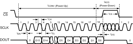 Figure 1. ADC161S626 Single Conversion Timing Diagram
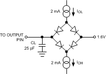 Figure 2. Timing Test Circuit
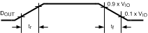 Figure 3. DOUT Rise and Fall Times
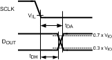 Figure 4. DOUT Hold and Access Times
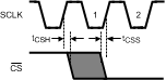 Figure 5. Valid CS Assertion Times
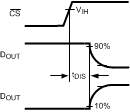 Figure 6. Voltage Waveform for tDIS
6.7 Typical Characteristics
VA = VIO = VREF = 5 V, fSCLK = 5 MHz, fSAMPLE = 250 kSPS, TA = +25°C, and fIN = 20 kHz unless otherwise stated.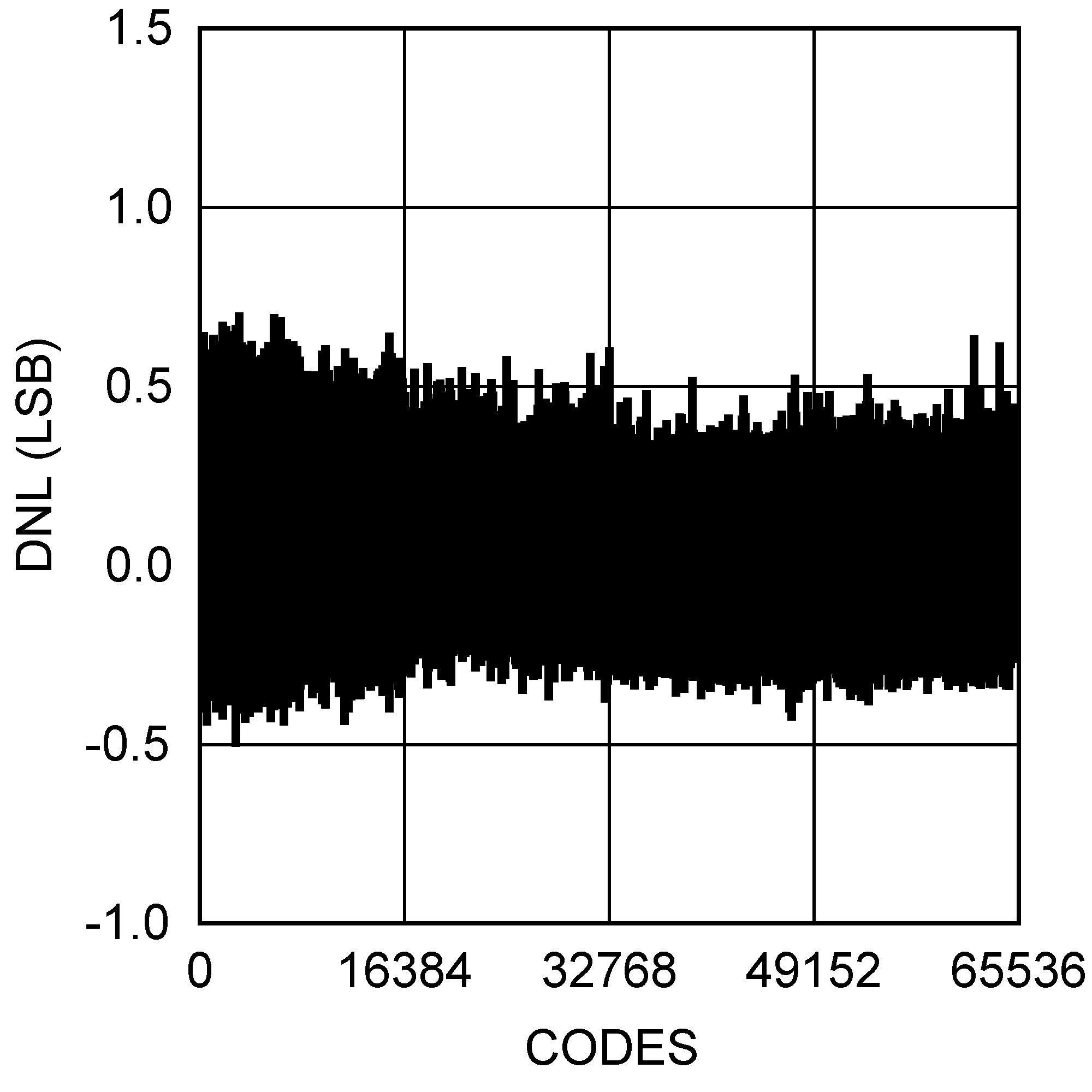 Figure 7. DNL - 250 kSPS
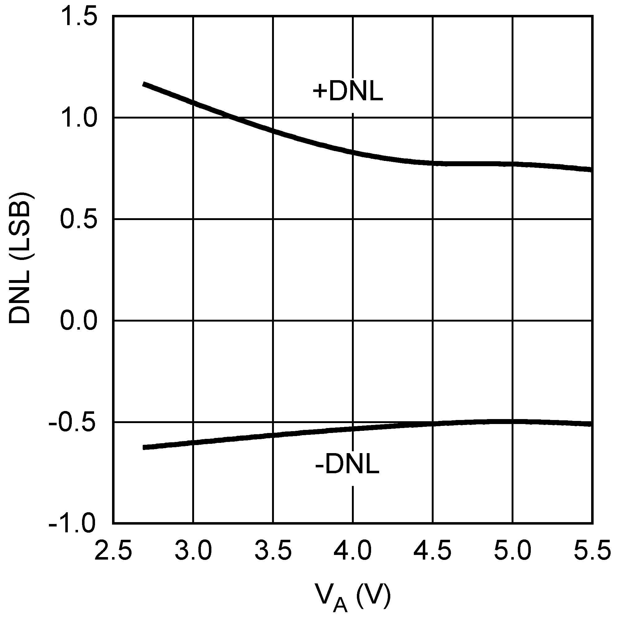 Figure 9. DNL vs. VA
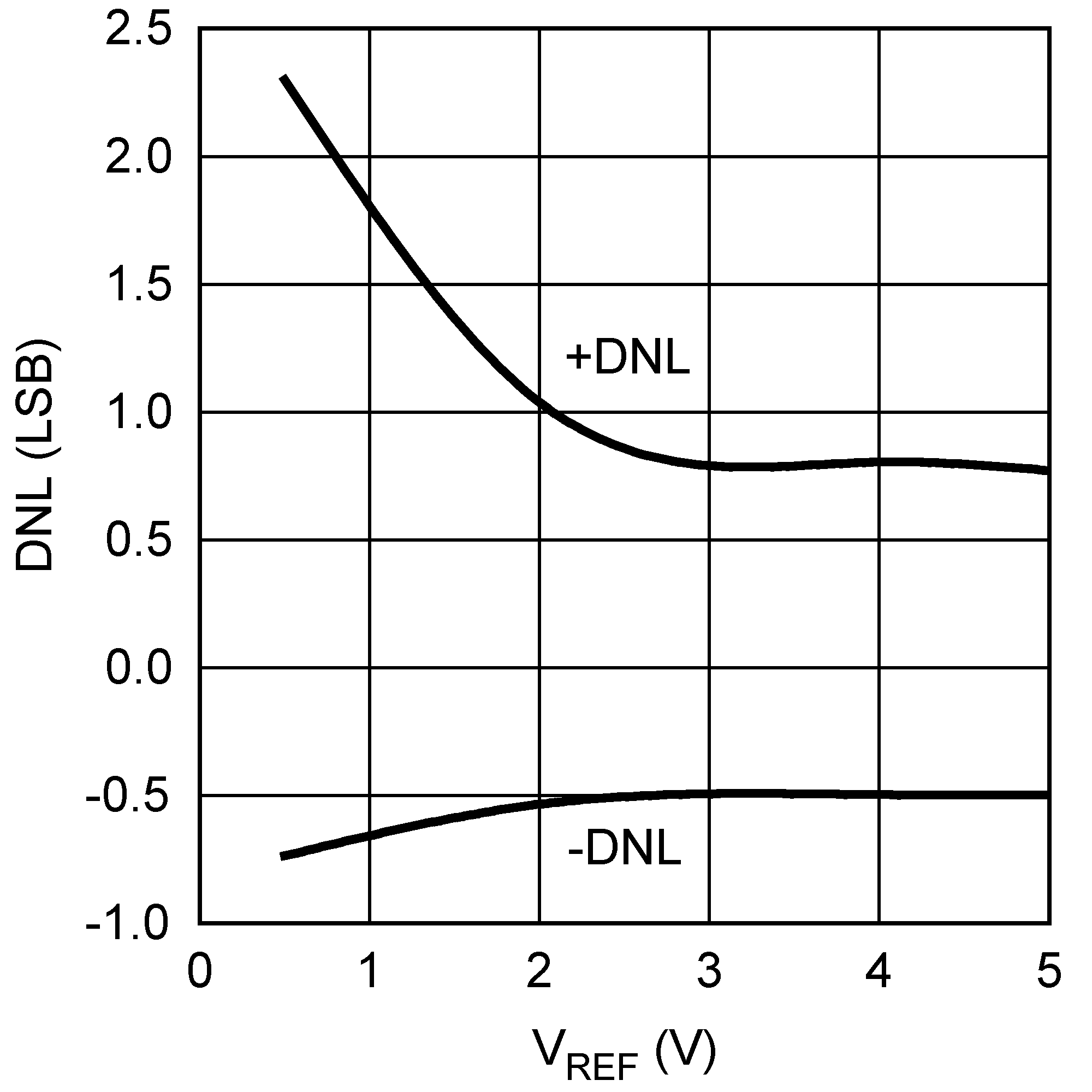 Figure 11. DNL vs. VREF
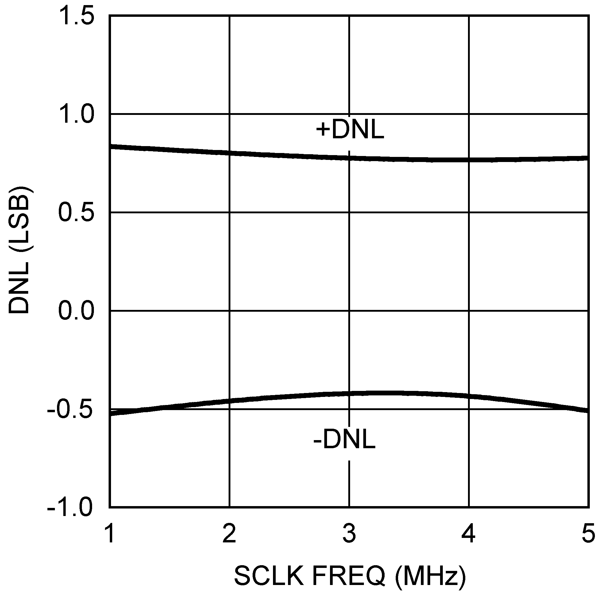 Figure 13. DNL vs. SCLK Frequency
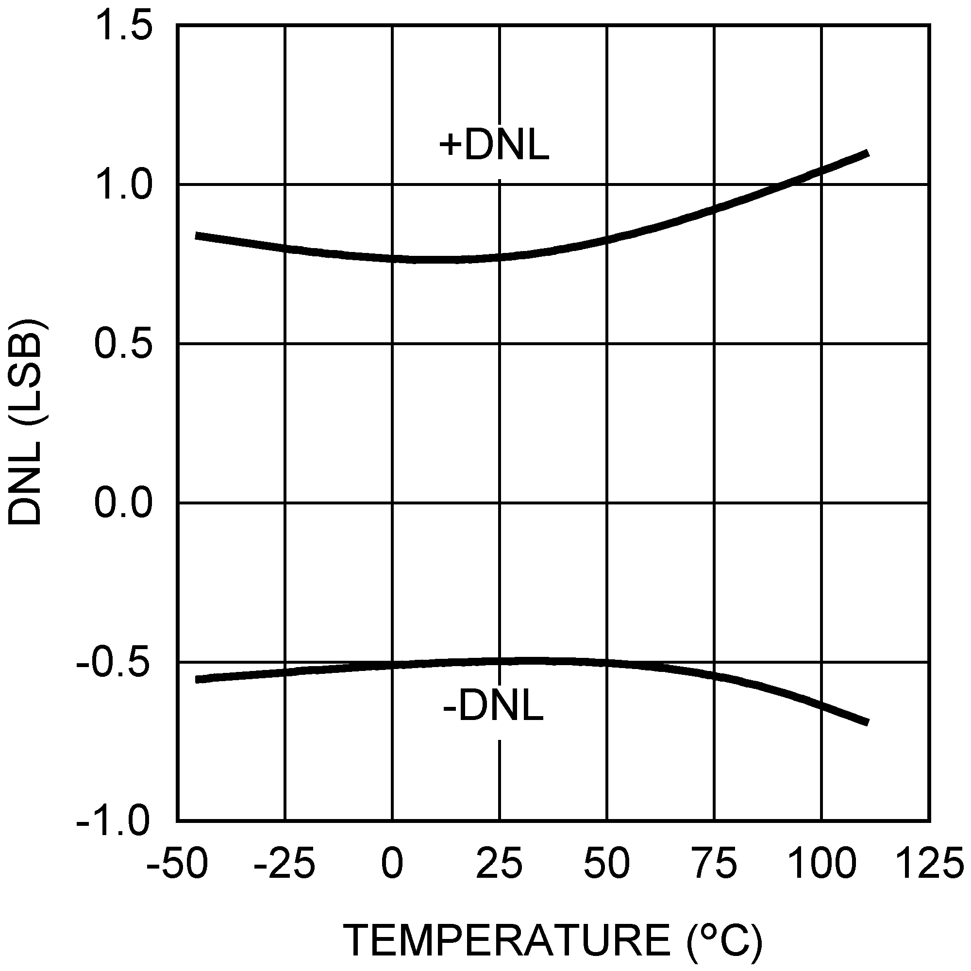 Figure 15. DNL vs. Temperature
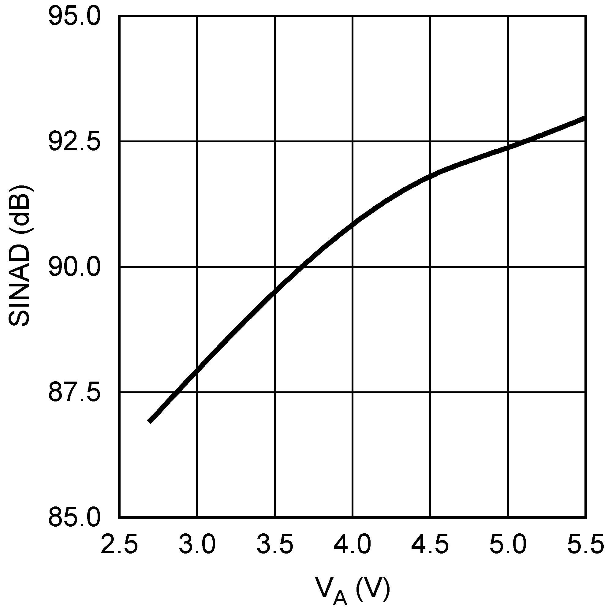 Figure 17. SINAD vs. VA
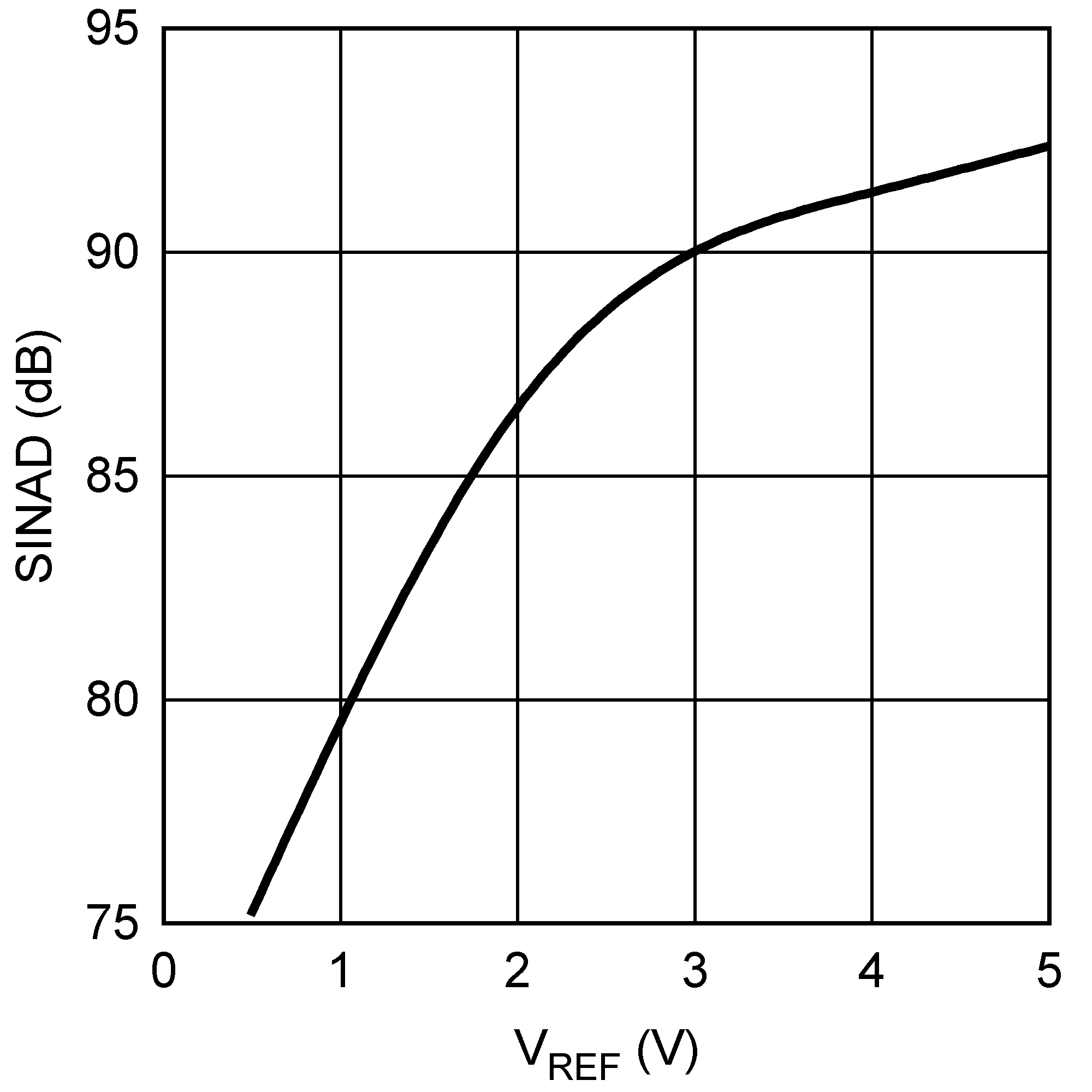 Figure 19. SINAD vs. VREF
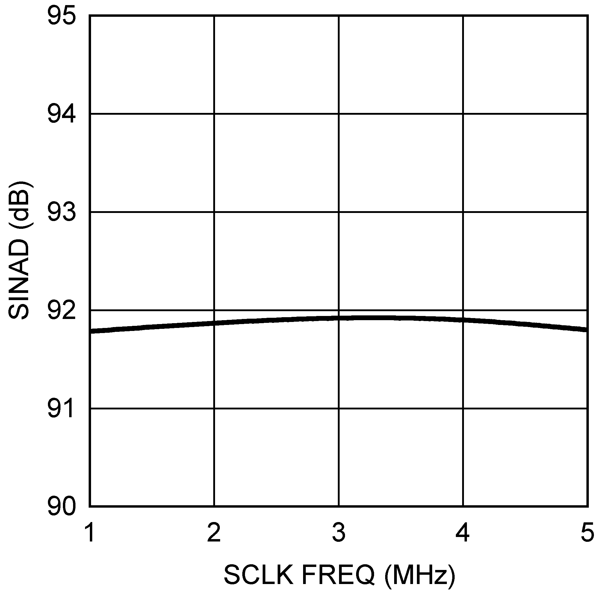 Figure 21. SINAD vs. SCLK Frequency
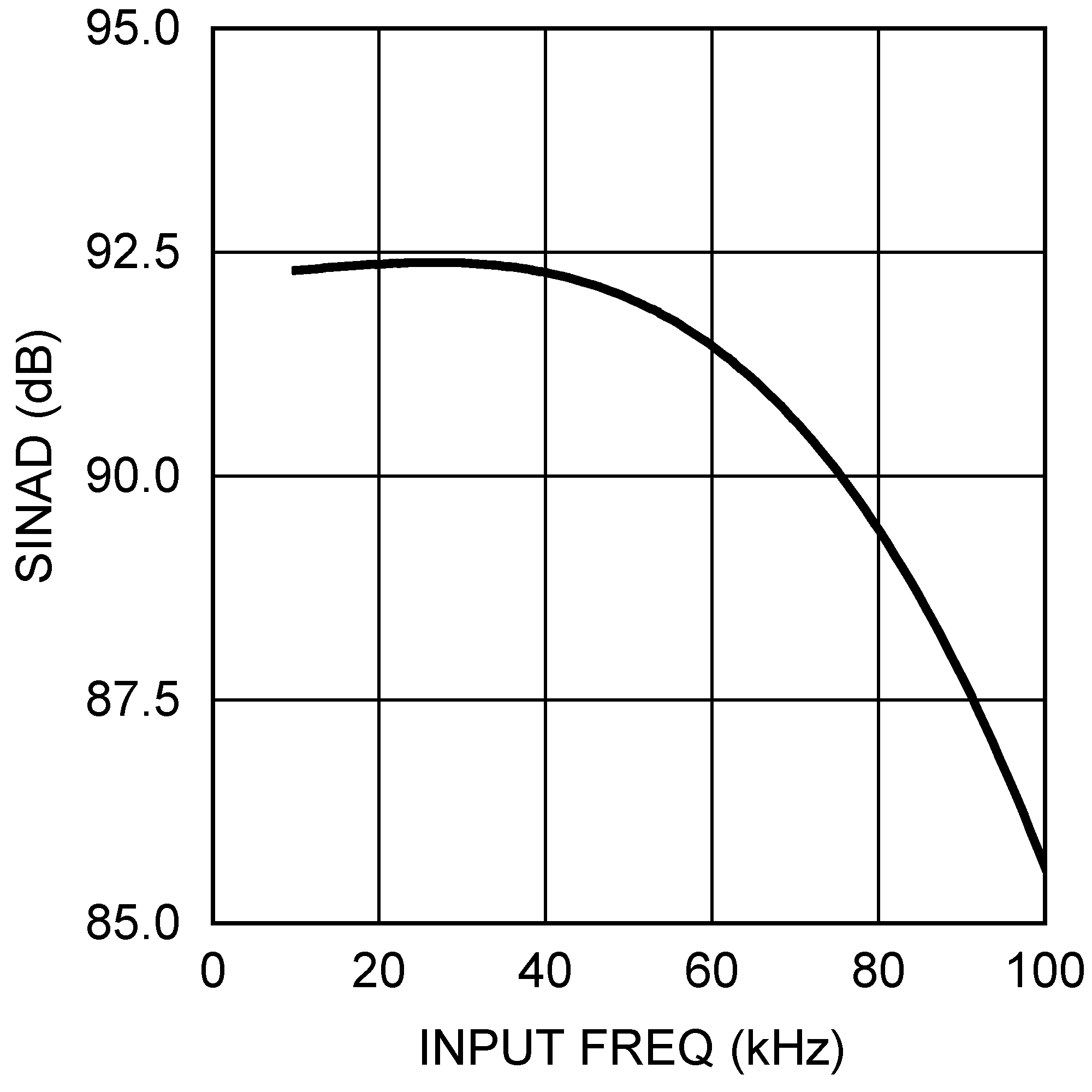 Figure 23. SINAD vs. INPUT Frequency
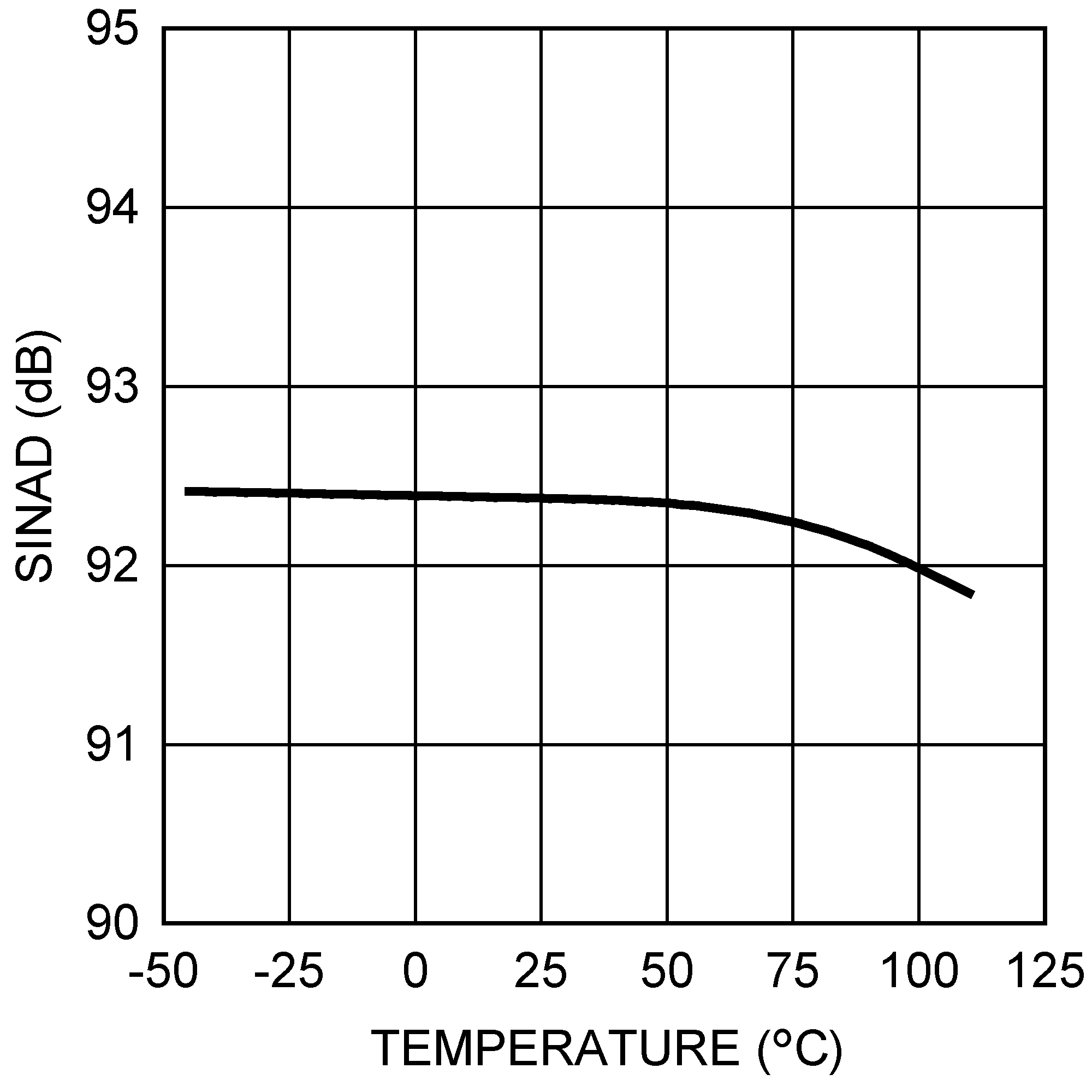 Figure 25. SINAD vs. Temperature
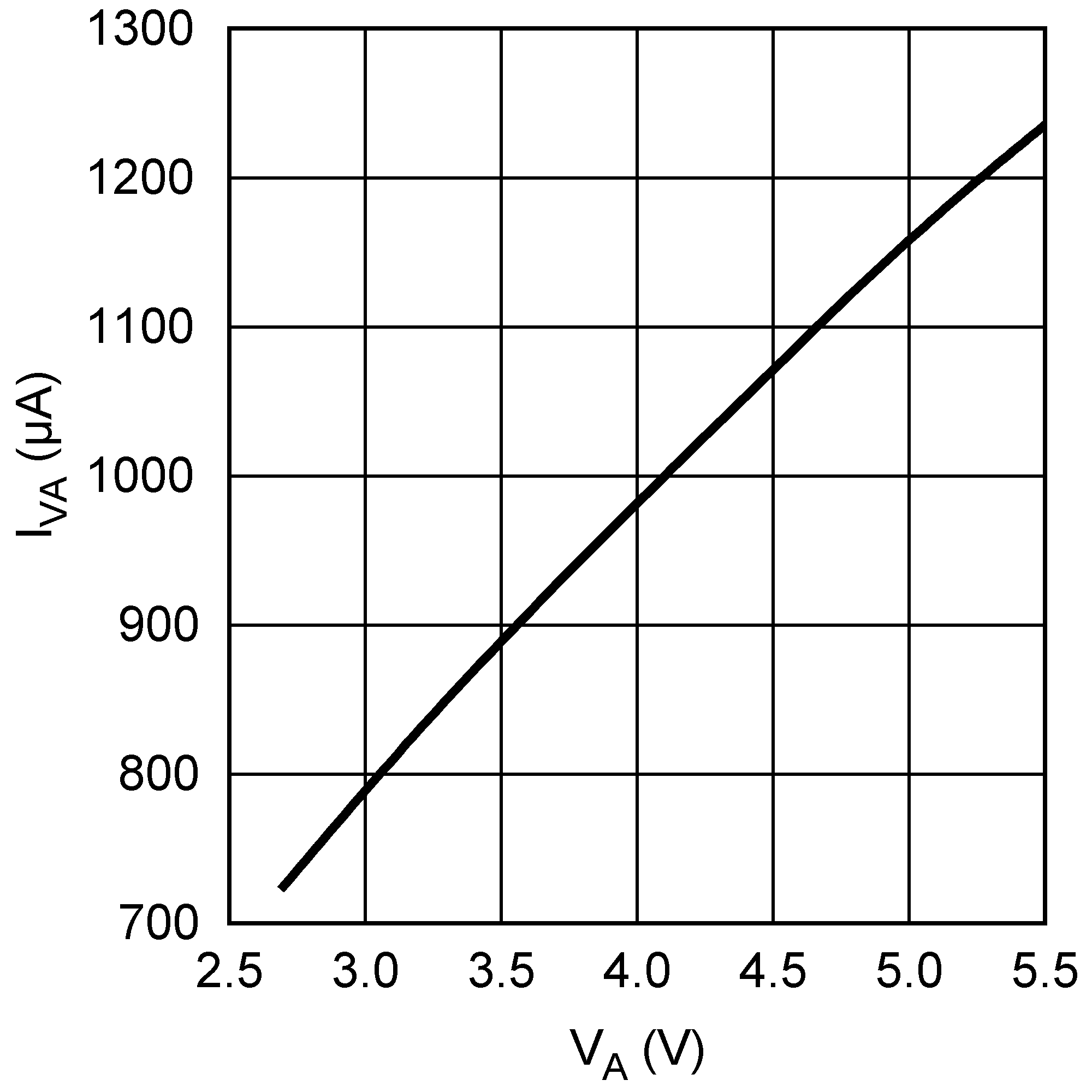 Figure 27. VA Current vs. VA
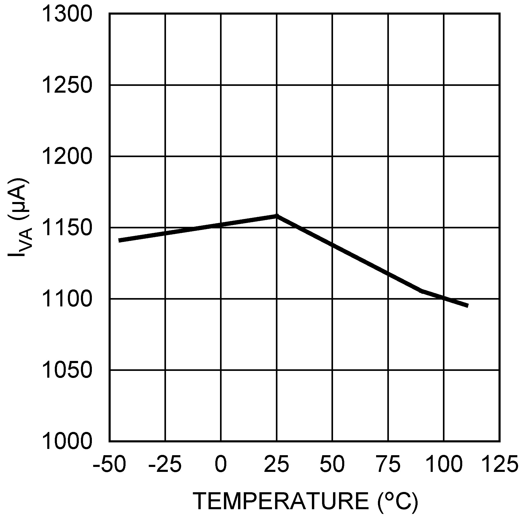 Figure 29. VA Current vs. Temperature
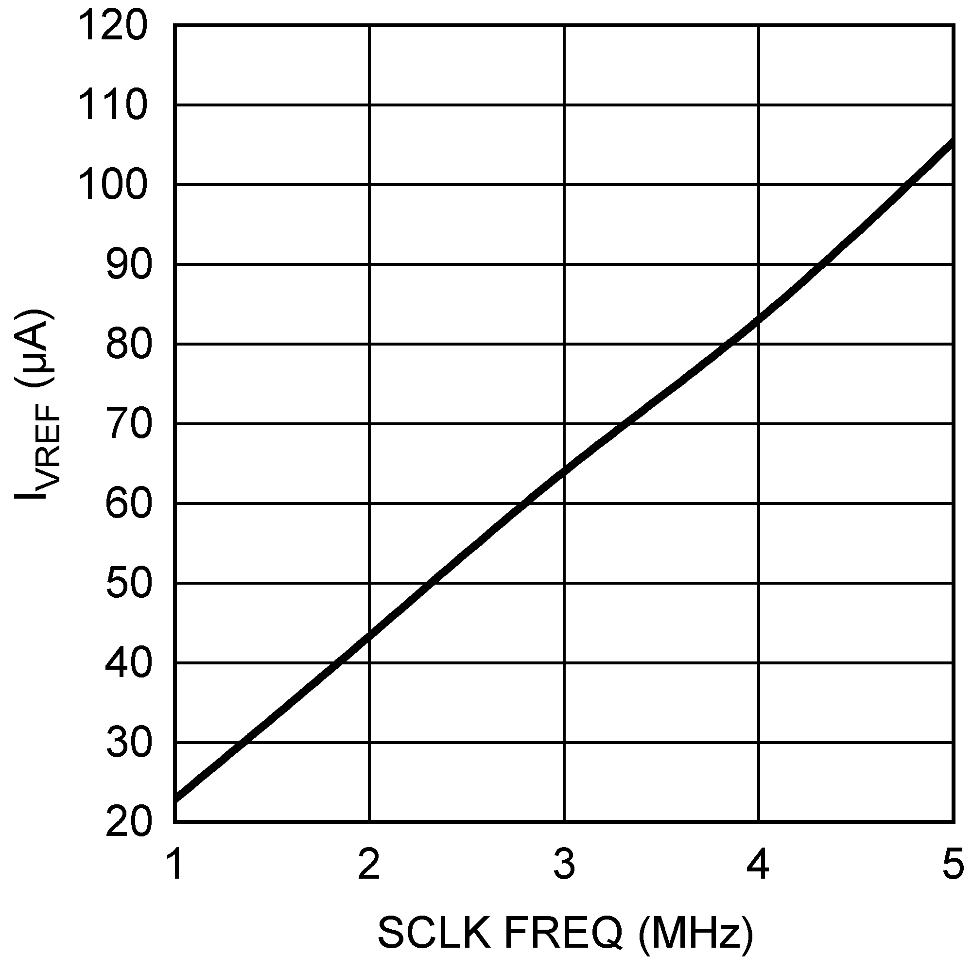 Figure 31. VREF Current vs. SCLK Frequency
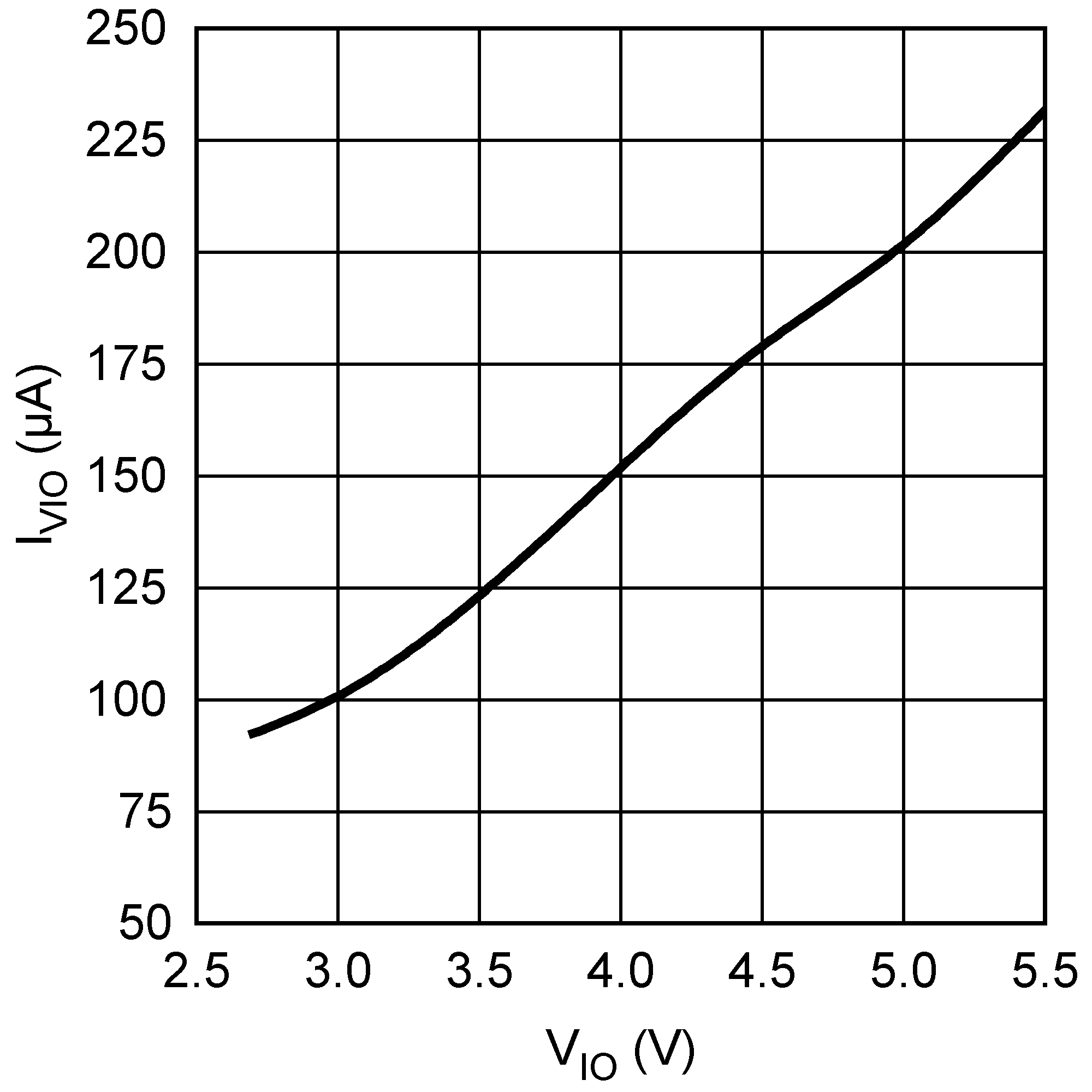 Figure 33. VIO Current vs. VIO
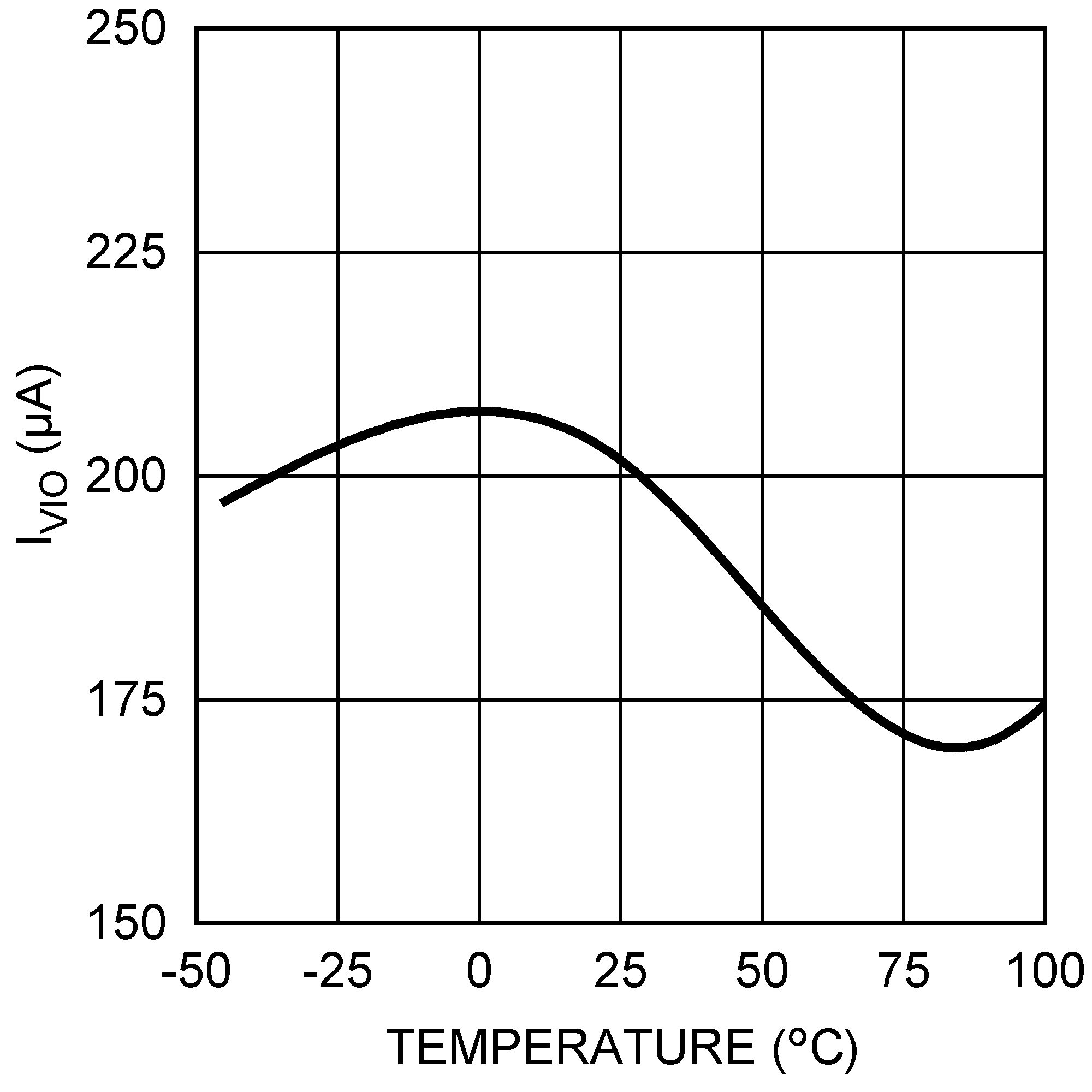 Figure 35. VIO Current vs. Temperature
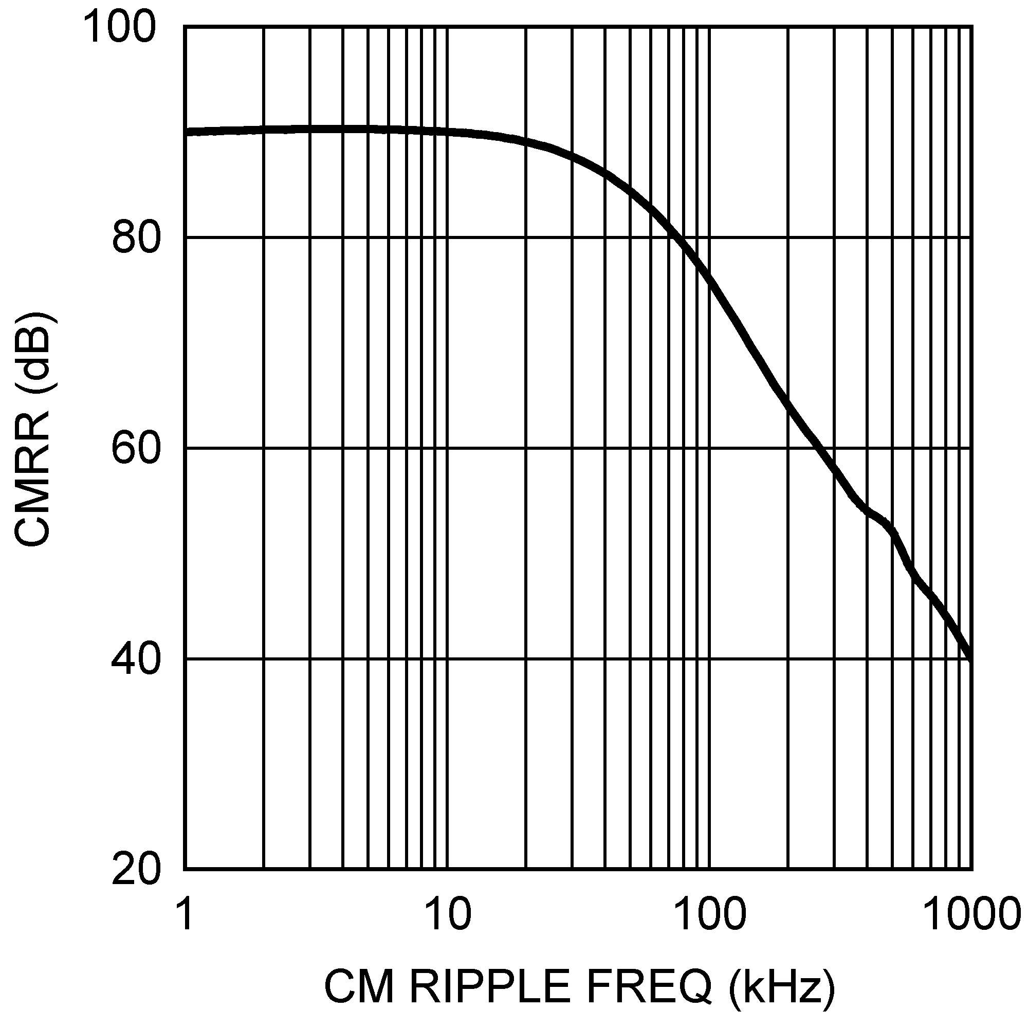 Figure 37. Analog Input CMRR vs. Frequency
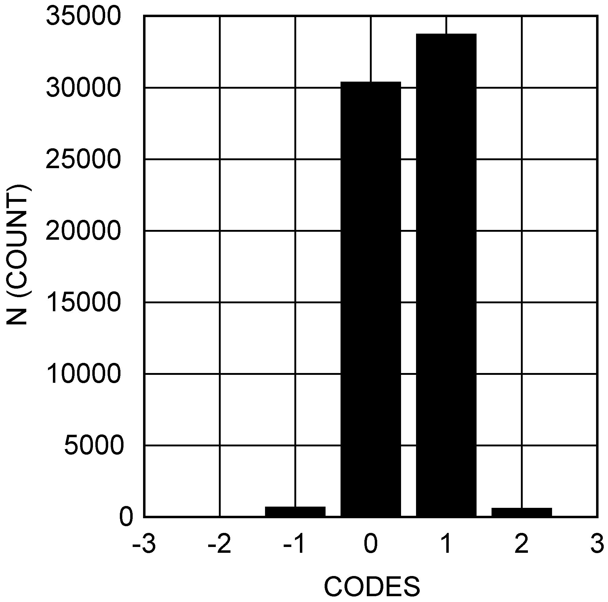 Figure 39. Noise Histogram at Code Transition
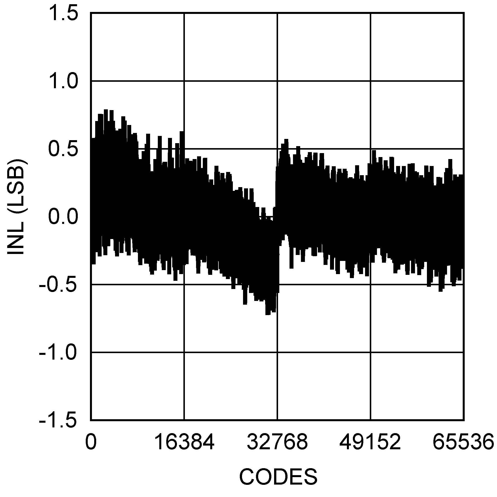 Figure 8. INL - 250 kSPS
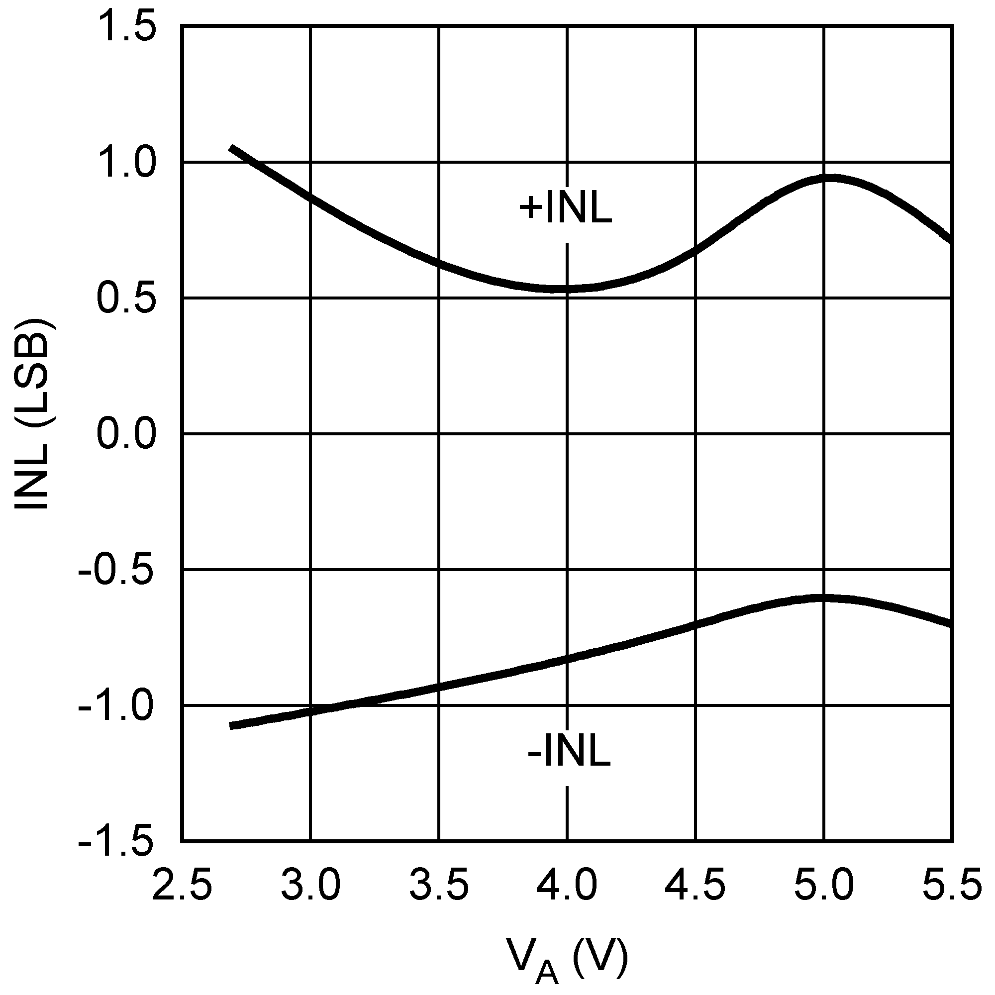 Figure 10. INL vs. VA
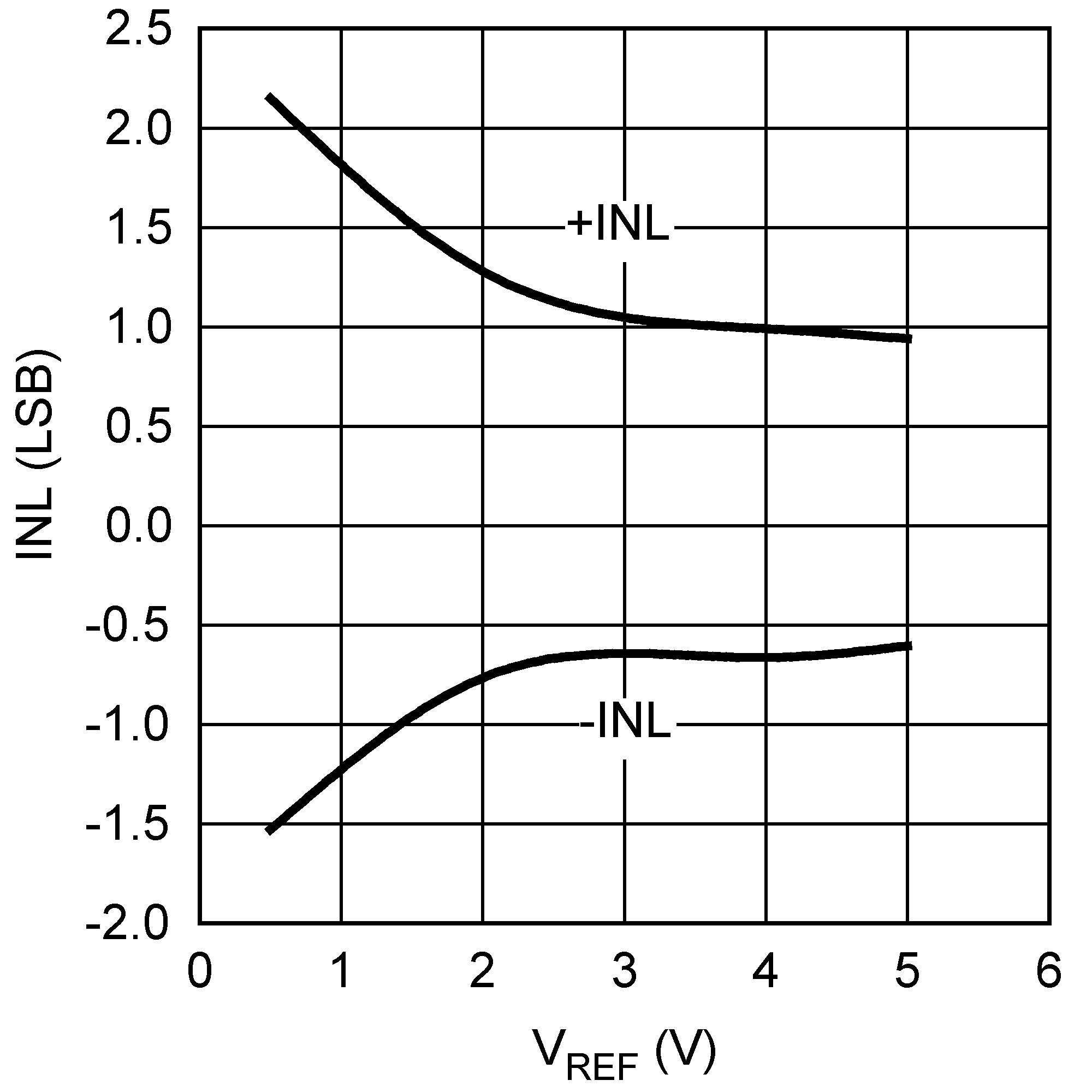 Figure 12. INL vs. VREF
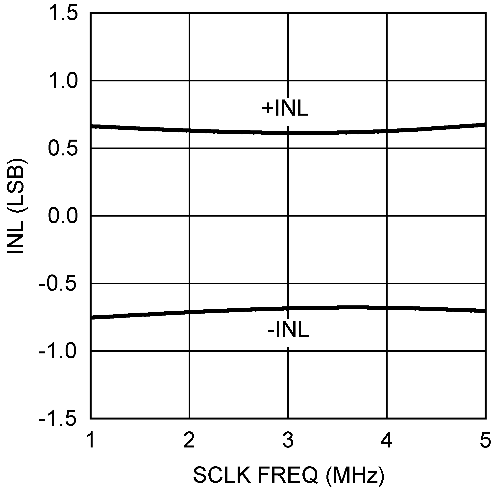 Figure 14. INL vs. SCLK Frequency
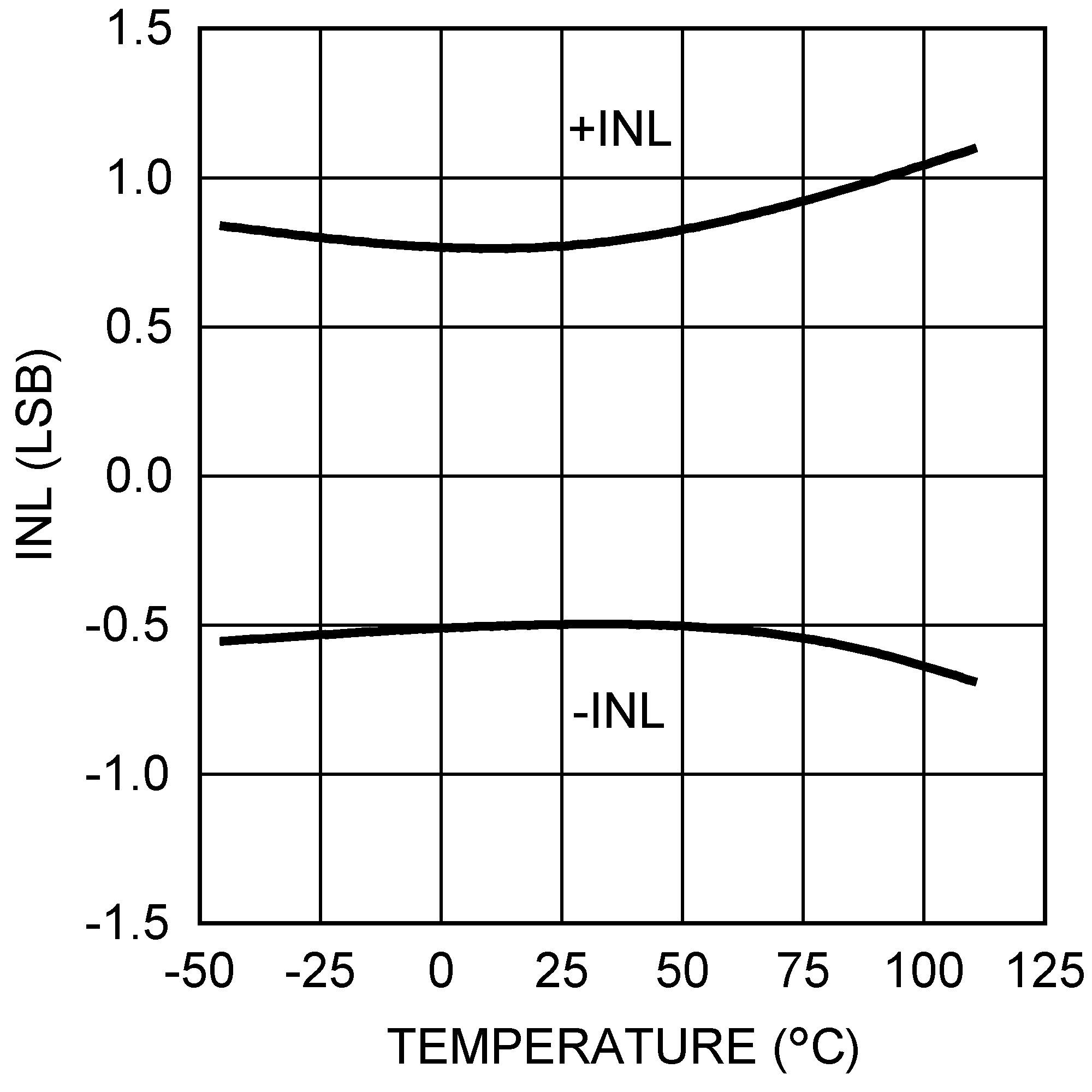 Figure 16. INL vs. Temperature
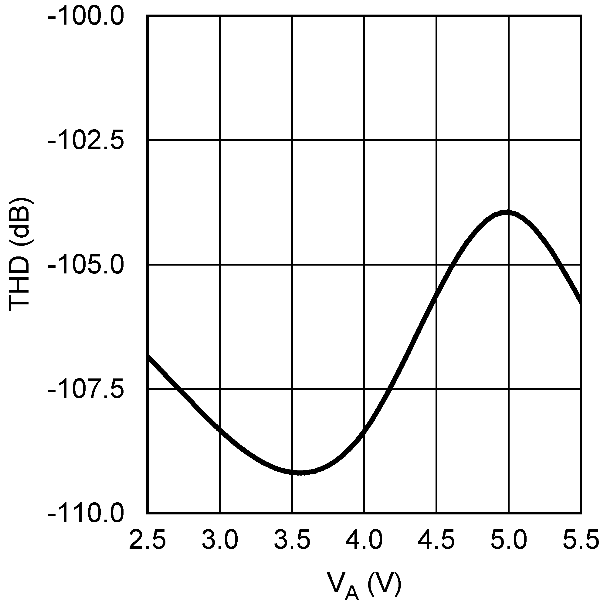 Figure 18. THD vs. VA
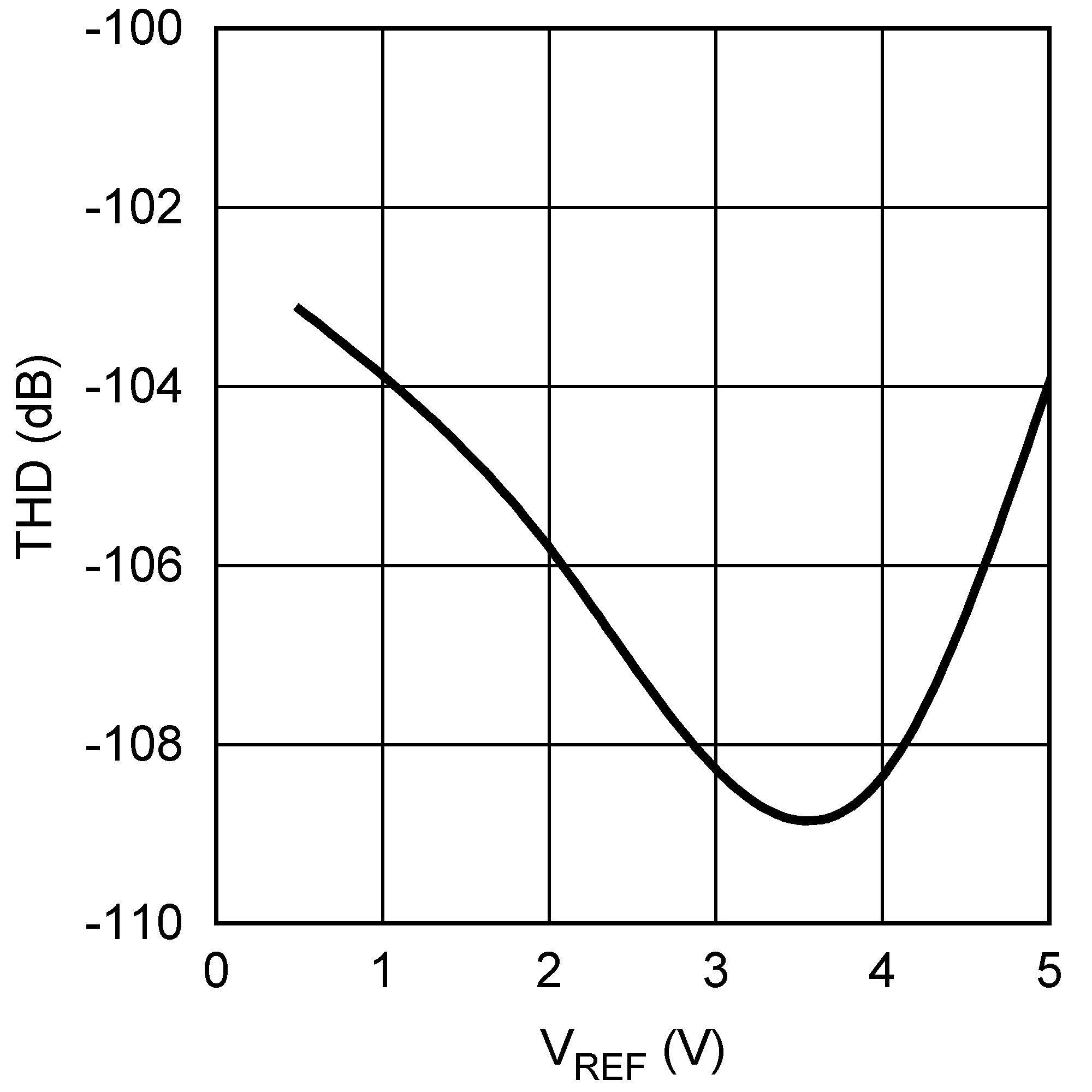 Figure 20. THD vs. VREF
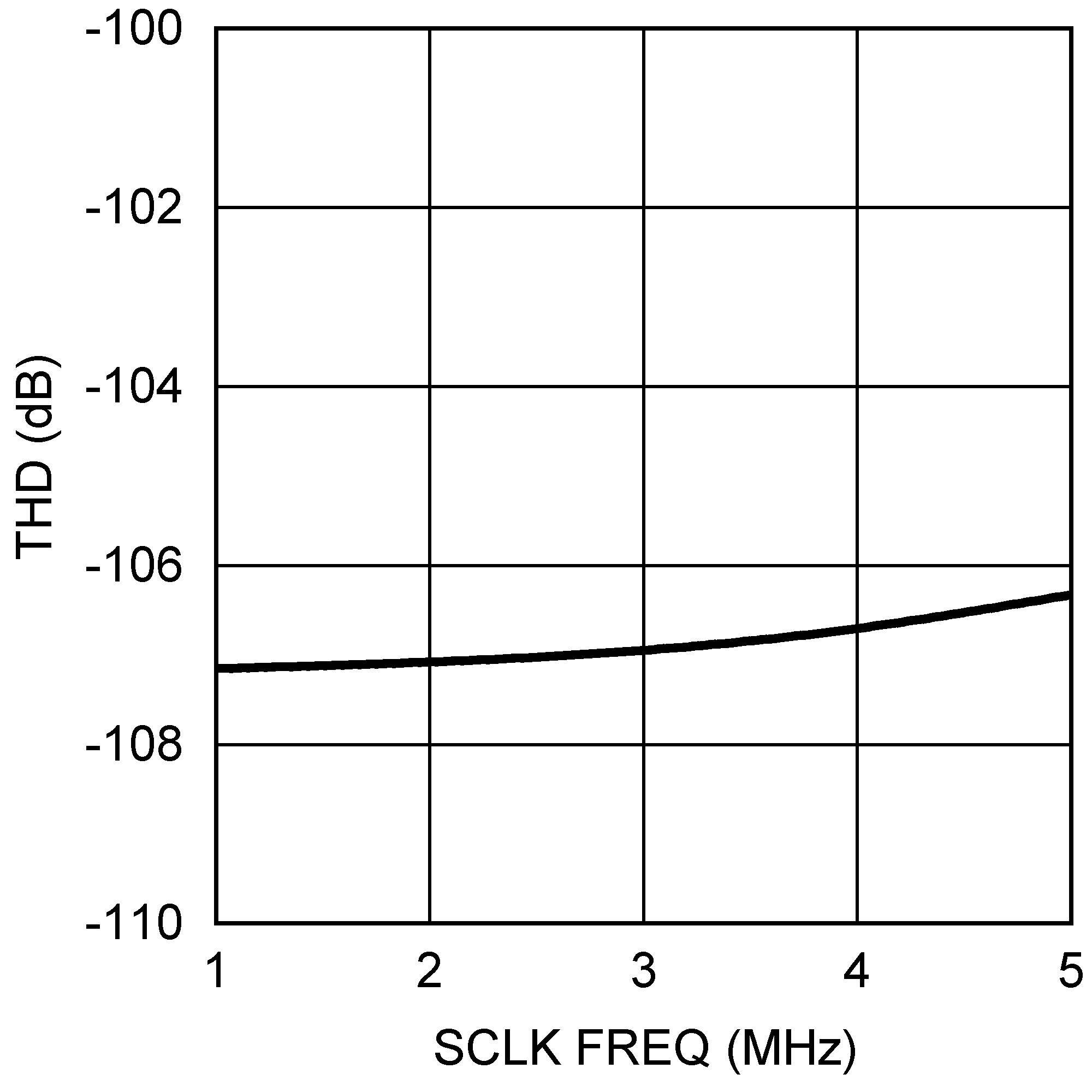 Figure 22. THD vs. SCLK Frequency
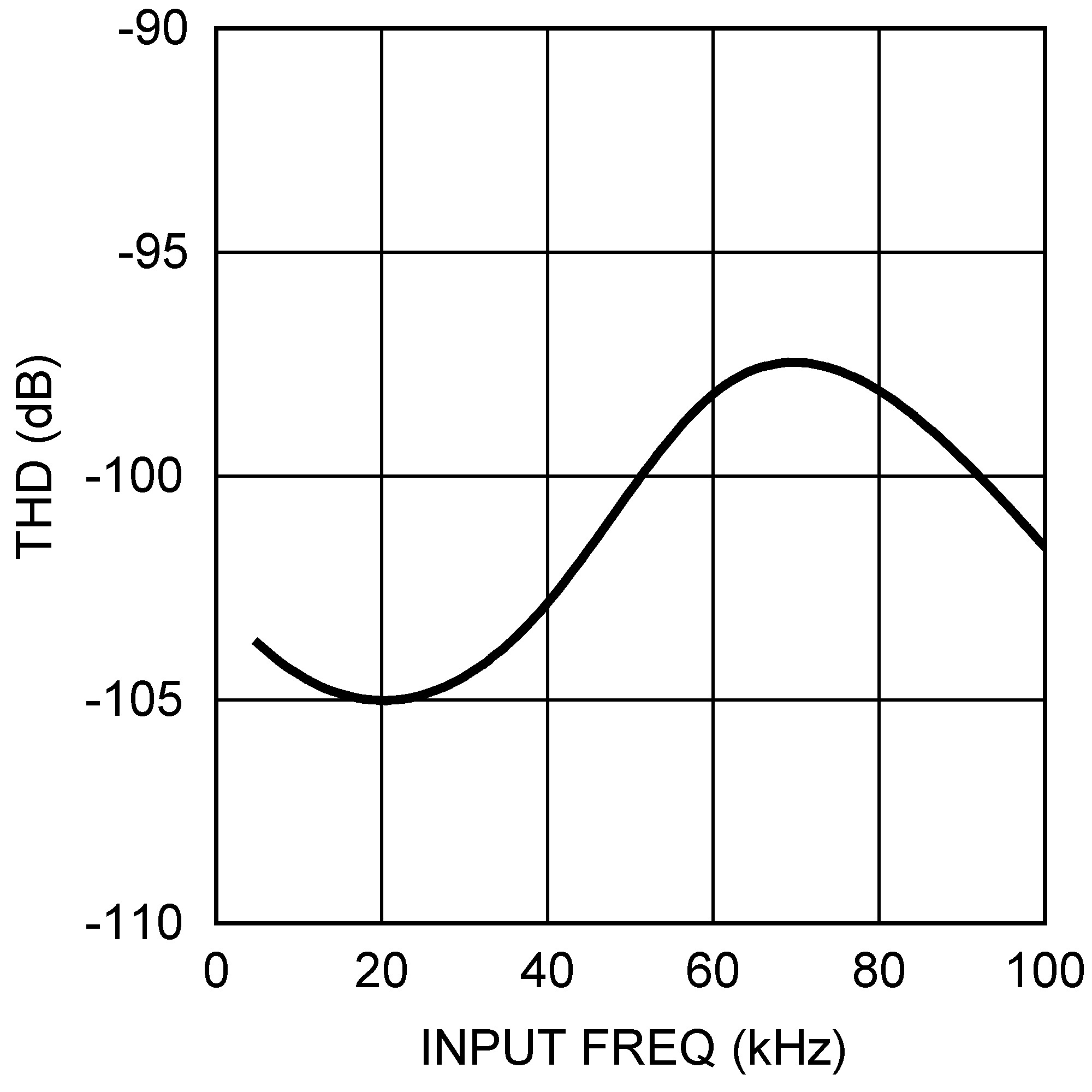 Figure 24. THD vs. INPUT Frequency
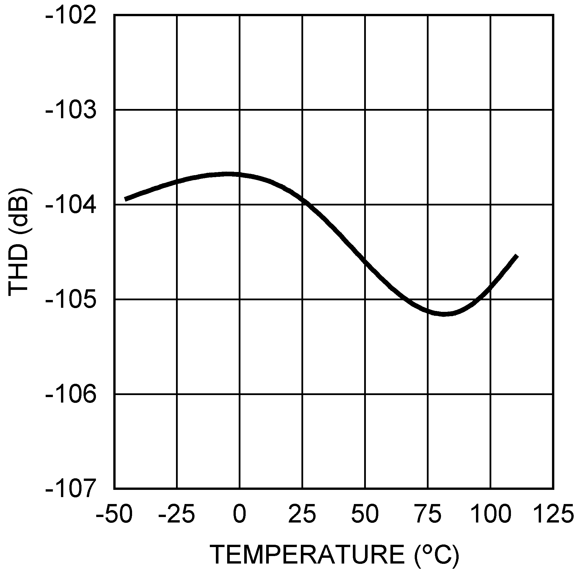 Figure 26. THD vs. Temperature
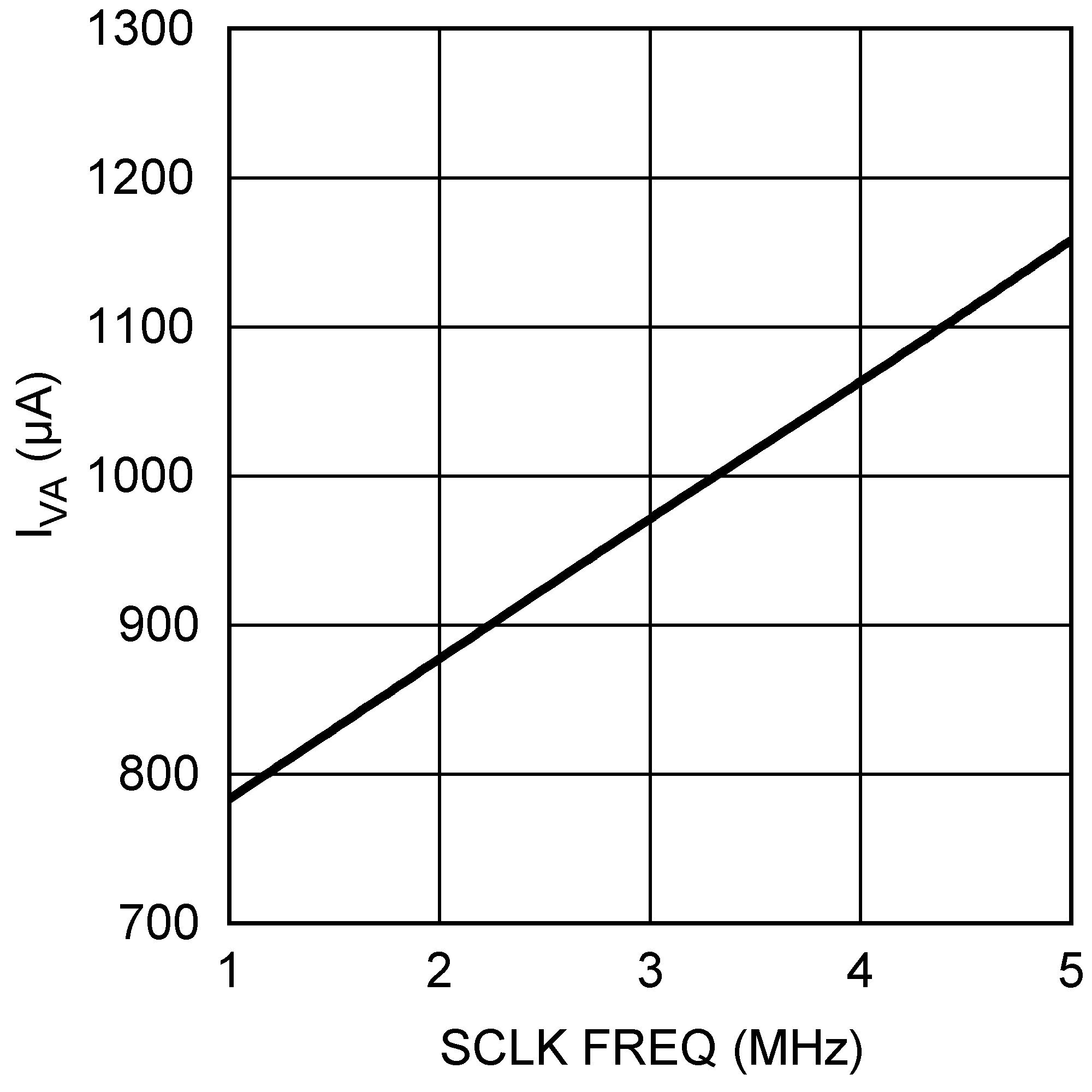 Figure 28. VA Current vs. SCLK Frequency
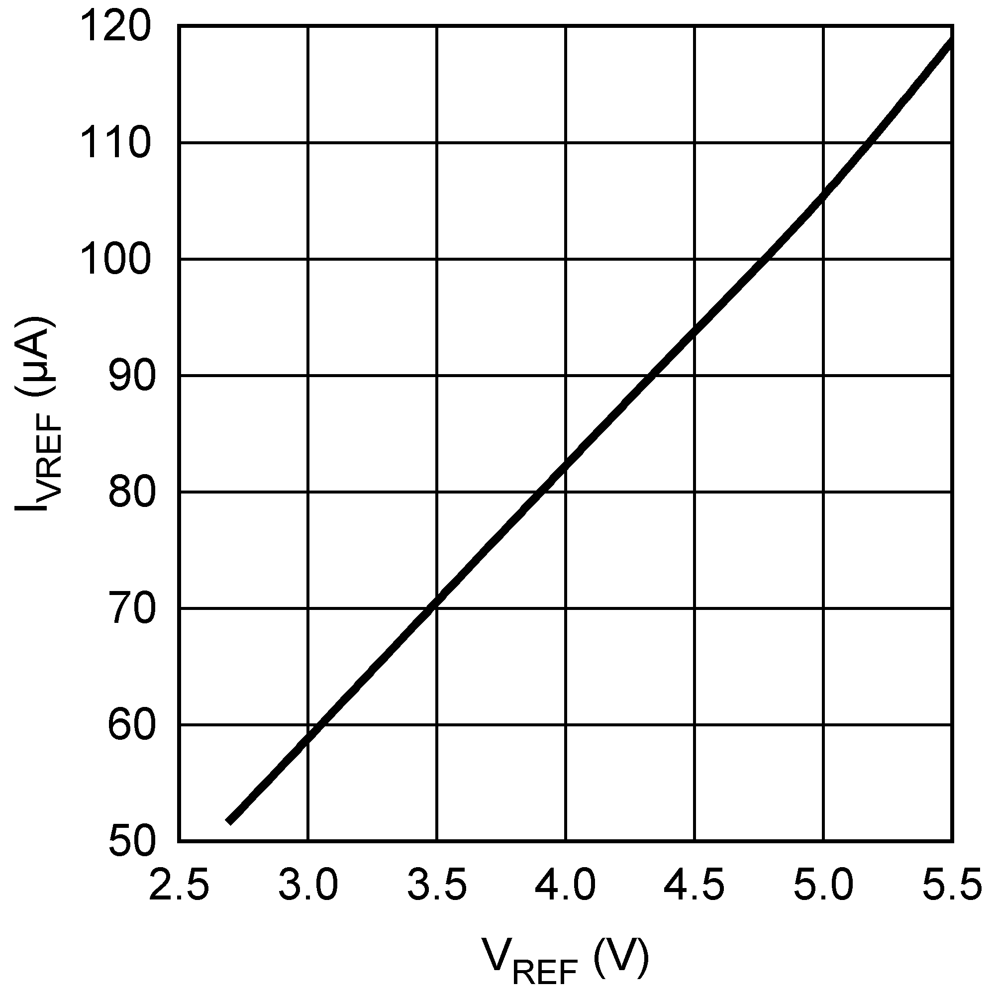 Figure 30. VREF Current vs. VREF
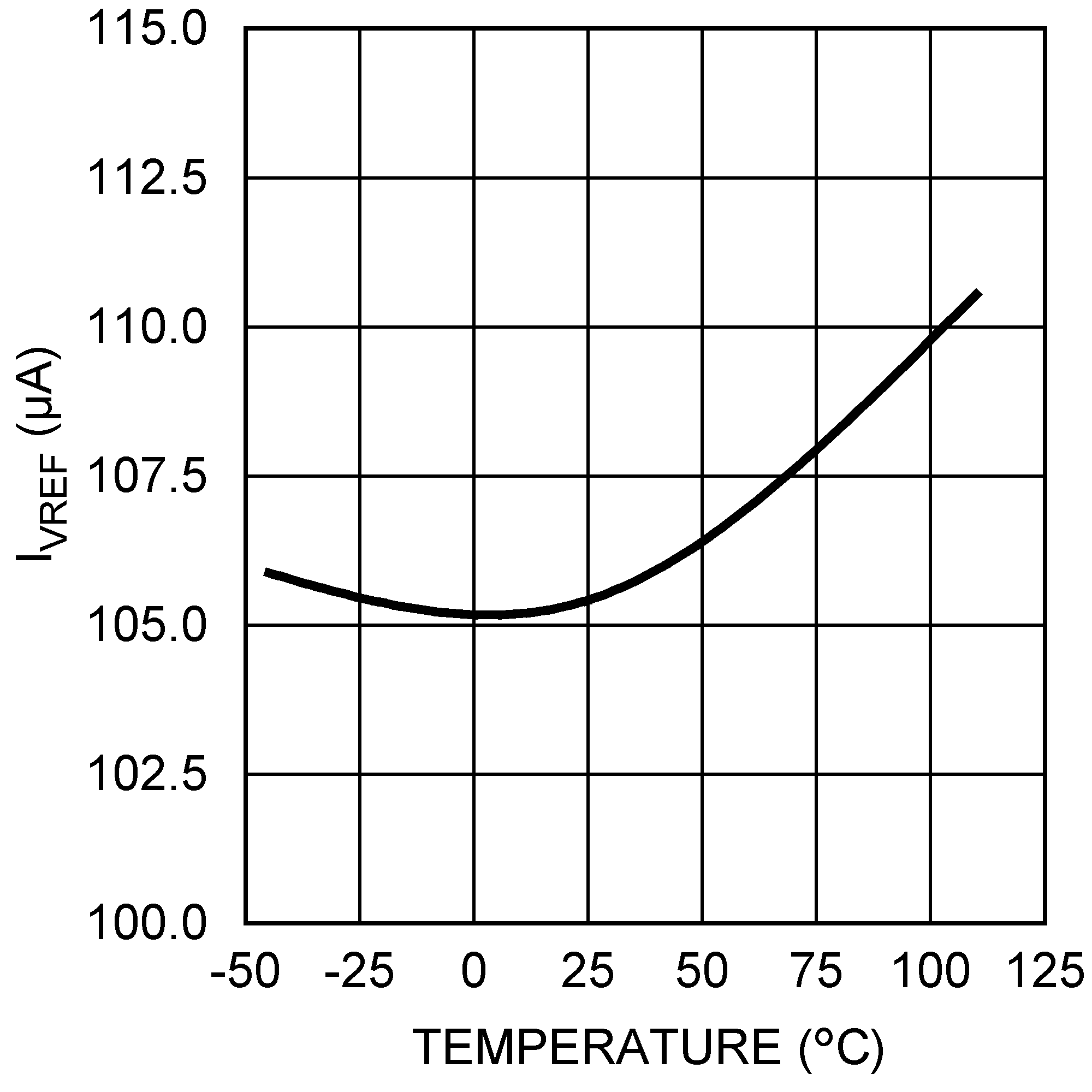 Figure 32. VREF Current vs. Temperature
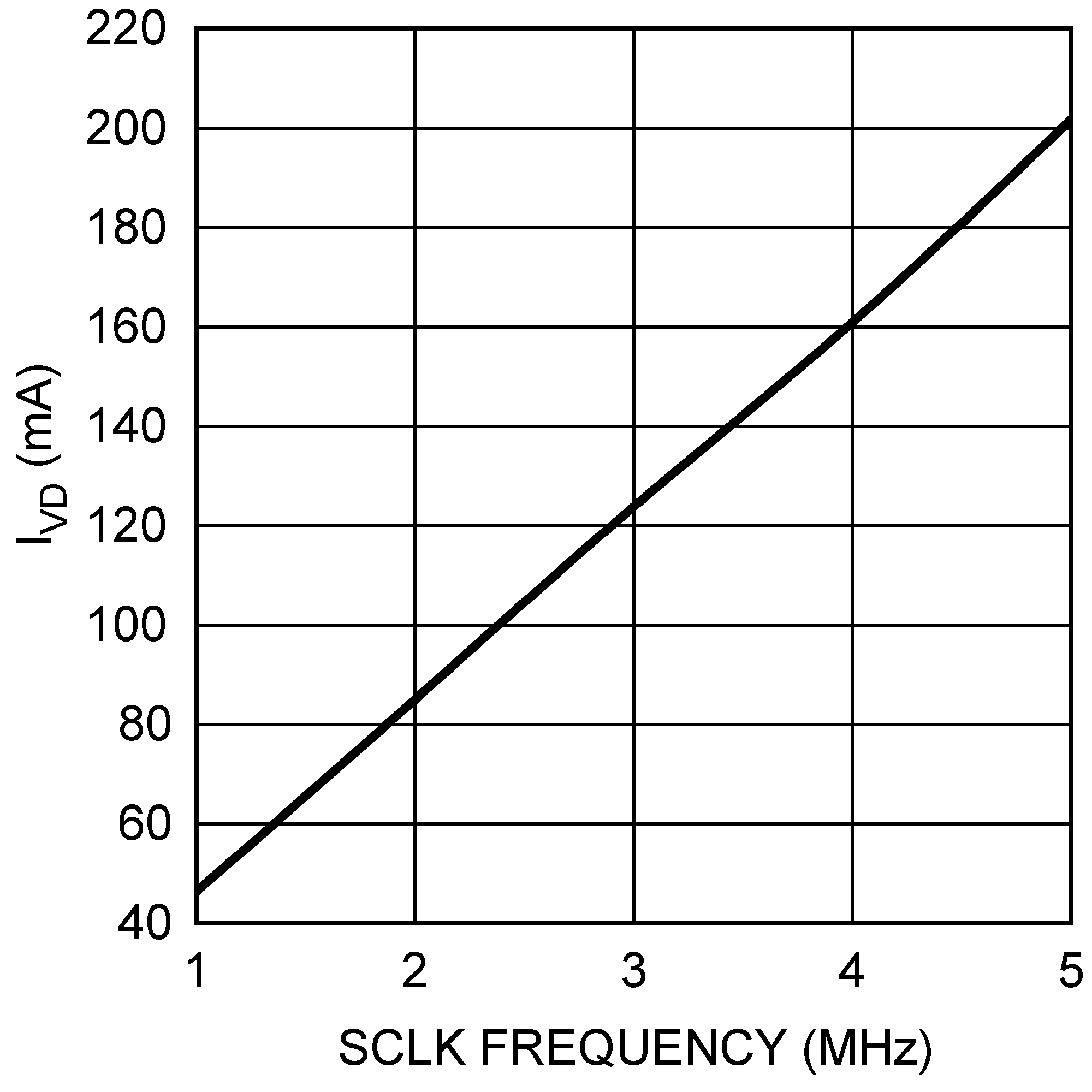 Figure 34. VIO Current vs. SCLK Frequency
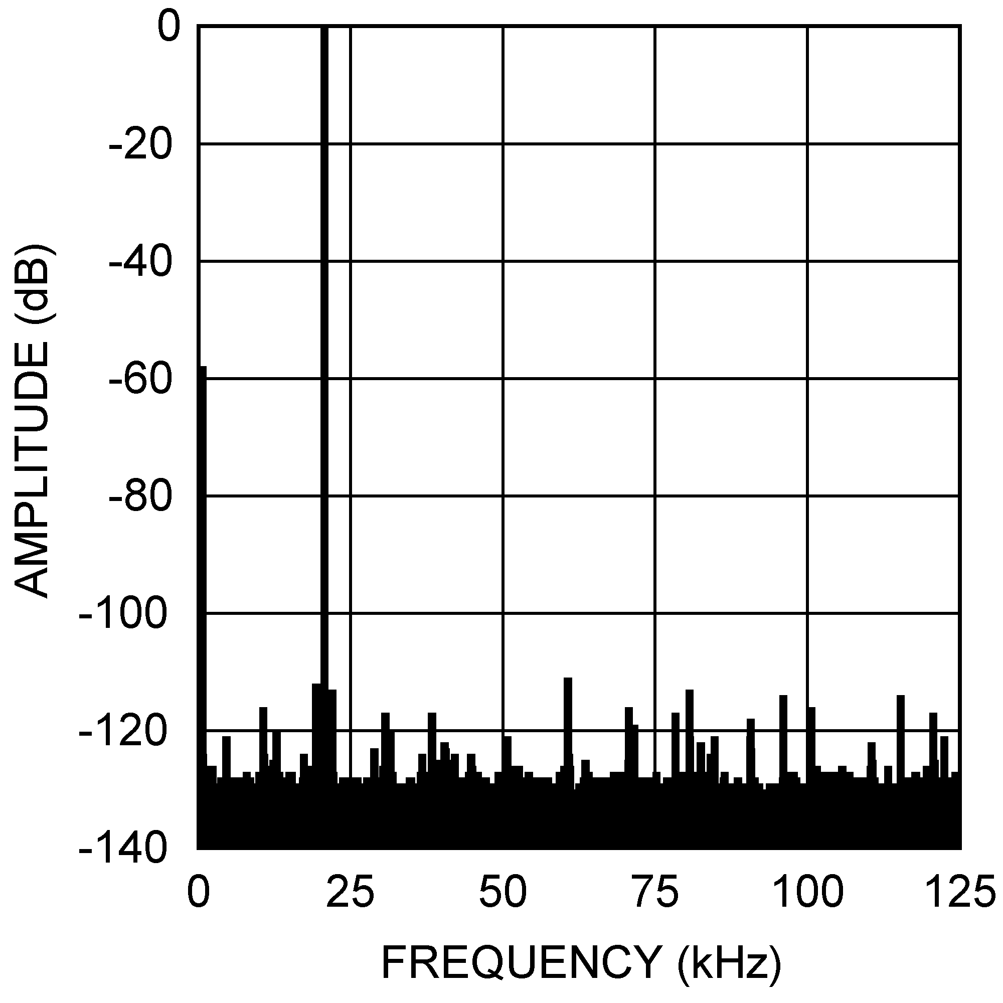 Figure 36. Spectral Response - 250 kSPS
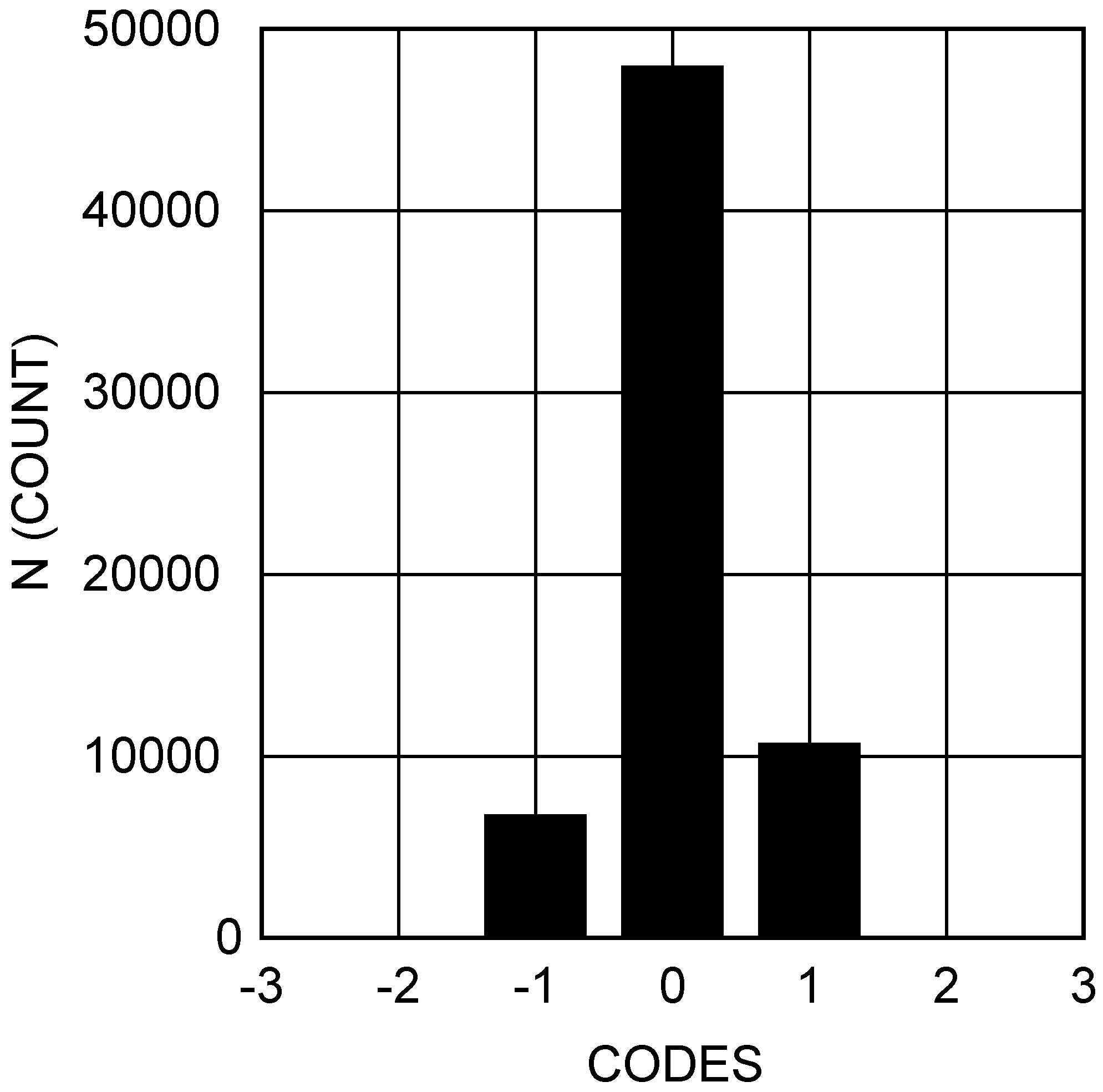 Figure 38. Noise Histogram at Code Center