SBAS580D May 2013 – March 2018 ADS7250 , ADS7850 , ADS8350
PRODUCTION DATA.
- 1 Features
- 2 Applications
- 3 Description
- 4 Revision History
- 5 Pin Configuration and Functions
-
6 Specifications
- 6.1 Absolute Maximum Ratings
- 6.2 ESD Ratings
- 6.3 Recommended Operating Conditions
- 6.4 Thermal Information
- 6.5 Electrical Characteristics: All Devices
- 6.6 Electrical Characteristics: ADS7250
- 6.7 Electrical Characteristics: ADS7850
- 6.8 Electrical Characteristics: ADS8350
- 6.9 Timing Requirements
- 6.10 Switching Characteristics
- 6.11 Typical Characteristics: ADS7250
- 6.12 Typical Characteristics: ADS7850
- 6.13 Typical Characteristics: ADS8350
- 6.14 Typical Characteristics: All Devices
- 7 Detailed Description
- 8 Application and Implementation
- 9 Power Supply Recommendations
- 10Layout
- 11Device and Documentation Support
- 12Mechanical, Packaging, and Orderable Information
Package Options
Mechanical Data (Package|Pins)
- RTE|16
Thermal pad, mechanical data (Package|Pins)
- RTE|16
Orderable Information
7.3.1 Reference
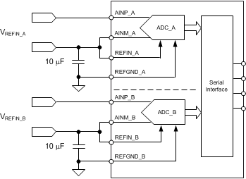
Each device has two simultaneous-sampling ADCs (ADC_A and ADC_B). ADC_A operates with reference voltage VREFIN_A and ADC_B operates with reference voltage VREFIN_B. These reference voltages must be provided on the REFIN_A and REFIN_B pins, respectively. REFIN_A and REFIN_B may be set to different values as per the application requirement.
As shown in Figure 49, decouple the REFIN_A and REFIN_B pins with the REFGND_A and REFGND_B pins, respectively, with individual 10-µF decoupling capacitors.
 Figure 49. Reference Block Diagram