SBAS580D May 2013 – March 2018 ADS7250 , ADS7850 , ADS8350
PRODUCTION DATA.
- 1 Features
- 2 Applications
- 3 Description
- 4 Revision History
- 5 Pin Configuration and Functions
-
6 Specifications
- 6.1 Absolute Maximum Ratings
- 6.2 ESD Ratings
- 6.3 Recommended Operating Conditions
- 6.4 Thermal Information
- 6.5 Electrical Characteristics: All Devices
- 6.6 Electrical Characteristics: ADS7250
- 6.7 Electrical Characteristics: ADS7850
- 6.8 Electrical Characteristics: ADS8350
- 6.9 Timing Requirements
- 6.10 Switching Characteristics
- 6.11 Typical Characteristics: ADS7250
- 6.12 Typical Characteristics: ADS7850
- 6.13 Typical Characteristics: ADS8350
- 6.14 Typical Characteristics: All Devices
- 7 Detailed Description
- 8 Application and Implementation
- 9 Power Supply Recommendations
- 10Layout
- 11Device and Documentation Support
- 12Mechanical, Packaging, and Orderable Information
Package Options
Mechanical Data (Package|Pins)
- RTE|16
Thermal pad, mechanical data (Package|Pins)
- RTE|16
Orderable Information
7.4.1 Serial Interface
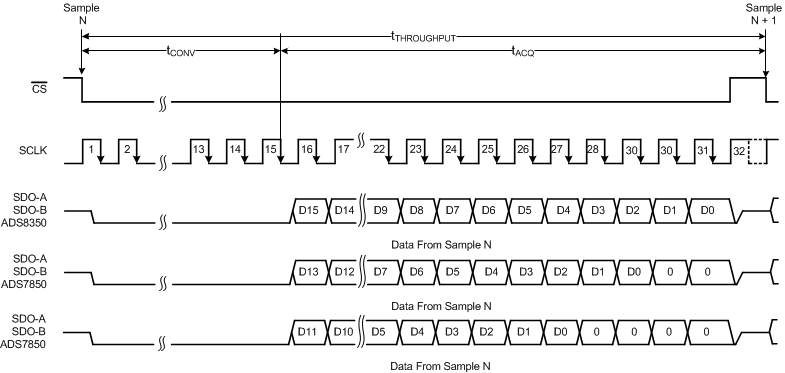
The devices support a simple, SPI-compatible serial interface to the external digital host. The CS signal defines one conversion and serial transfer frame. A frame starts with a CS falling edge and ends with a CS rising edge. The SDO_A and SDO_B pins output the ADC_A and ADC_B conversion results, respectively. Figure 52 shows a detailed timing diagram for these devices.
 Figure 52. Serial Interface Timing Diagram
A CS falling edge brings the serial data bus out of 3-state and also outputs a '0' on the SDO_A and SDO_B pins. The device converts the sampled analog input during the next 14 clocks. SDO_A and SDO_B read '0' during this period. The sample-and-hold circuit goes back into sample mode on the 15th SCLK falling edge and the MSBs of ADC_A and ADC_B are output on SDO_A and SDO_B, respectively. The subsequent clock edges are used to shift out the conversion result using the serial interface, as shown in Table 2. Output data are in binary twos complement format. A CS rising edge ends the frame and puts the serial bus into 3-state.
Table 2. Data Launch Edge
| DEVICE | PIN | LAUNCH EDGE | |||||||||||||
|---|---|---|---|---|---|---|---|---|---|---|---|---|---|---|---|
| CS ↓ | SCLK | CS ↑ | |||||||||||||
| ↓1 | … | ↓14 | ↓15 | … | ↓26 | ↓27 | ↓28 | ↓29 | ↓30 | ↓31 | … | ||||
| ADS8350 | SDO-A | 0 | 0 | … | 0 | D15_A | … | D4_A | D3_A | D2_A | D1_A | D0_A | 0 | … | Hi-Z |
| SDO-B | 0 | 0 | … | 0 | D15_B | … | D4_B | D3_B | D2_B | D1_B | D0_B | 0 | … | Hi-Z | |
| ADS7850 | SDO-A | 0 | 0 | … | 0 | D13_A | … | D2_A | D1_A | D0_A | 0 | 0 | 0 | … | Hi-Z |
| SDO-B | 0 | 0 | … | 0 | D13_B | … | D2_B | D1_B | D0_B | 0 | 0 | 0 | … | Hi-Z | |
| ADS7250 | SDO-A | 0 | 0 | … | 0 | D11_A | … | D0_A | 0 | 0 | 0 | 0 | 0 | … | Hi-Z |
| SDO-B | 0 | 0 | … | 0 | D11_B | … | D0_B | 0 | 0 | 0 | 0 | 0 | … | Hi-Z | |