SBAS580D May 2013 – March 2018 ADS7250 , ADS7850 , ADS8350
PRODUCTION DATA.
- 1 Features
- 2 Applications
- 3 Description
- 4 Revision History
- 5 Pin Configuration and Functions
-
6 Specifications
- 6.1 Absolute Maximum Ratings
- 6.2 ESD Ratings
- 6.3 Recommended Operating Conditions
- 6.4 Thermal Information
- 6.5 Electrical Characteristics: All Devices
- 6.6 Electrical Characteristics: ADS7250
- 6.7 Electrical Characteristics: ADS7850
- 6.8 Electrical Characteristics: ADS8350
- 6.9 Timing Requirements
- 6.10 Switching Characteristics
- 6.11 Typical Characteristics: ADS7250
- 6.12 Typical Characteristics: ADS7850
- 6.13 Typical Characteristics: ADS8350
- 6.14 Typical Characteristics: All Devices
- 7 Detailed Description
- 8 Application and Implementation
- 9 Power Supply Recommendations
- 10Layout
- 11Device and Documentation Support
- 12Mechanical, Packaging, and Orderable Information
Package Options
Mechanical Data (Package|Pins)
- RTE|16
Thermal pad, mechanical data (Package|Pins)
- RTE|16
Orderable Information
7.4.2 Short-Cycling, Frame Abort, and Reconversion Feature
Referring to Table 2, the ADS8350 requires a minimum of 31 SCLK falling edges between the beginning and end of the frame to complete the 16-bit data transfer, the ADS7850 requires a minimum of 29 SCLK falling edges between the beginning and end of the frame to complete the 14-bit data transfer, and the ADS7250 requires a minimum of 27 SCLK falling edges between the beginning and end of the frame to complete the 12-bit data transfer. However, CS can be brought high at any time during the frame to abort the frame or to short-cycle the converter.
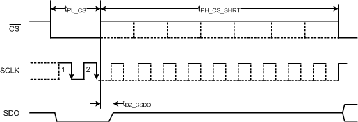
As shown in Figure 53, if CS is brought high before the 15th SCLK falling edge, the device aborts the conversion and starts sampling the new analog input signal.
 Figure 53. Frame Aborted before 15th SCLK Falling Edge
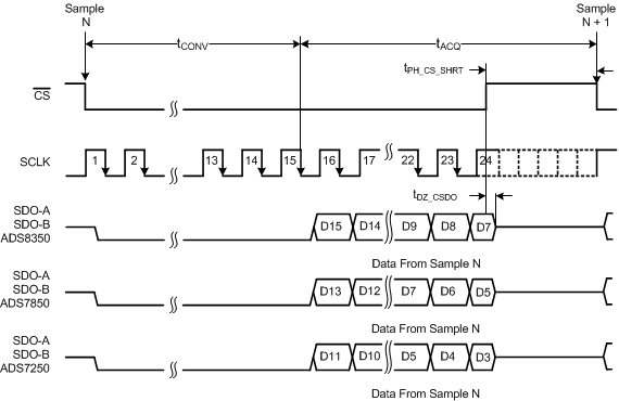
If CS is brought high after the 15th SCLK falling edge (as shown in Figure 54), the output data bits latched into the digital host before this CS rising edge are still valid data corresponding to sample N.
 Figure 54. Frame Aborted after 15th SCLK Falling Edge
After aborting the current frame, CS must be kept high for tPH_CS_SHRT to ensure that the minimum acquisition time (tACQ) is provided for the next conversion.