SLUSBE4B January 2014 – June 2014
PRODUCTION DATA.
- 1 Features
- 2 Applications
- 3 Description
- 4 Simplified Diagram
- 5 Revision History
- 6 Pin Configuration and Functions
- 7 Specifications
-
8 Detailed Description
- 8.1 Overview
- 8.2 Functional Block Diagram
- 8.3
Feature Description
- 8.3.1 A6 Coil Specification
- 8.3.2 EMI Shield
- 8.3.3 I2C Interface
- 8.3.4 Active or Passive Wake-up State
- 8.3.5 Smart Key or Immobilizer Handling
- 8.3.6 Option Select Pins
- 8.3.7 LED Modes
- 8.3.8 Foreign Object Detection (FOD) and Parasitic Metal Object Detect (PMOD) CalibrationForeign Object Detection (FOD) and Parasitic Metal Object Detect (PMOD) Calibration description.
- 8.3.9 Shut Down via External Thermal Sensor or Trigger
- 8.3.10 Fault Handling and Indication
- 8.3.11 Power Transfer Start Signal
- 8.3.12 Power-On Reset
- 8.3.13 External Reset, RESET Pin
- 8.3.14 Trickle Charge and CS100
- 8.3.15 Over-Voltage Protection Over-Voltage Protection section.
- 8.4 Device Functional Modes
- 9 Applications and Implementation
- 10Power Supply Recommendations
- 11Layout
- 12Device and Documentation Support
- 13Mechanical, Packaging, and Orderable Information
Package Options
Mechanical Data (Package|Pins)
- RGZ|48
Thermal pad, mechanical data (Package|Pins)
- RGZ|48
Orderable Information
8 Detailed Description
8.1 Overview
The principle of wireless power transfer is simply an open cored transformer consisting of transmitter (Tx) and receiver (Rx) coils. The transmitter coil and electronics are typically built into a charger pad and the receiver coil and electronics are typically built into a portable device, such as a cell-phone.
When the receiver coil is positioned on the transmitter coil, magnetic coupling occurs once the transmitter coil is driven. The flux is coupled into the secondary coil which induces a voltage and current flows. The secondary voltage is rectified, and power can be transferred effectively to a load, wirelessly. Power transfer can be managed through any of various familiar closed-loop control schemes.
The bq500414Q sends an analog ping to detect the presence of a receiver on the pad. An external enable trigger or proximity detector can also be used to provide the means of detecting the presence of a receiver. The detector can output an enable signal to the regulator supplying the bq500414Q and the device powers up, or the enable signal can start the Tx via I2C command. Once the bq500414Q is active, it pings the three coils sequentially to detect and power up the Rx. Once the Rx is powered up, it sends the communication packages to the Tx. The package information can be fetched by the Tx through demodulating the COMM feedback signal, which is a scaled version of primary coil voltage. The COMM feedback signal is multiplexed through analog switches and is synchronized to the coil being driven. To select the best coil match, the bq500414Q looks for the strongest COMM signal. Note that only one coil is driven at a time. The driven coil is tolerant of slight misalignment of the Rx while power is being transferred. Actually displacing the Rx to an adjacent coil while charging is allowable, the sequential ping sequence and detection to determine the best matching coil to drive continues to repeat. bq500414Q provides I2C interface to support some read and write commands, which can also be used to start the Tx and temporarily shift the Tx operating frequency.
8.2 Functional Block Diagram
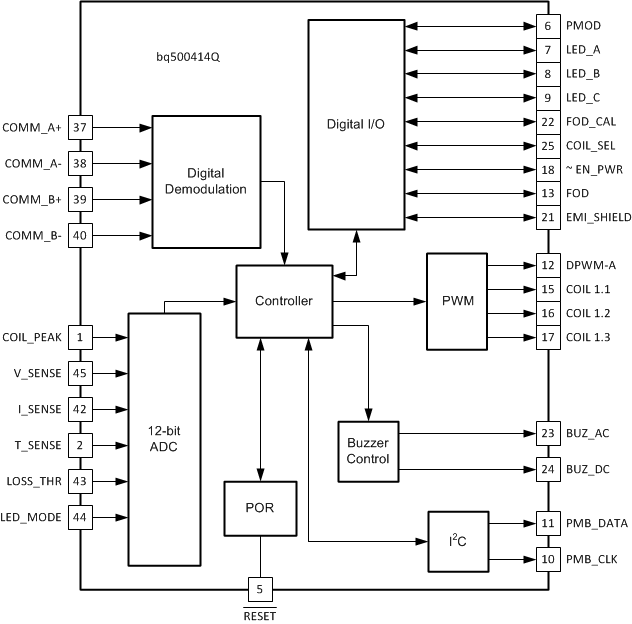
8.3 Feature Description
8.3.1 A6 Coil Specification
bq500414Q supports WPC A6 transmitter type. The coil and matching capacitor specification for the A6 transmitter has been established by WPC standard. This is fixed and cannot be changed on the transmitter side.
The bq500414Q is primarily intended to drive a 3 coil array but it can also be used to drive a single coil or two coils. For single coil operation, the other coils and associated electronics are simply omitted.
Schematics and BOM can be found on the product folder at www.ti.com.
For a current list of coil vendors please see:
- bqTESLA Transmitter Coil Vendors, SLUA649
8.3.2 EMI Shield
TI recommends using a PCB based Electromagnetic Interference (EMI) shield to improve the EMI performance. The shield needs to be grounded. Pin 21 is used to indicate if EMI shield is in use. See product folder at www.ti.com for additional information on reference designs and applications.
8.3.3 I2C Interface
The bq500414Q supports read and write commands via I2C, as well as firmware upgrade. This could help the host controller monitor system information, control output power, and temporarily shift the Tx operating frequency.
The slave address assigned to the bq500414Q has been hardcoded to 20 (decimal). The hardware can support 100-kHz, 400-kHz, or 1-MHz I2C operation. Contact Texas Instruments for additional information on I2C interface.
8.3.4 Active or Passive Wake-up State
At power up, the bq500414Q will read EN_PWR pin voltage. If it is low, the bq500414Q device will be in active wake-up state. It will send a analog ping to detect if a compatible Rx is present and then sends a digital ping to power up the Rx. If the EN_PWR pin voltage is high, the bq500414Q will be in a passive wake-up state and considers that the SHUTDOWN command is issued. It will not send any analog ping or digital ping to detect the presence Rx, until the SHUTDOWN command is disabled through I2C. Once the SHUTDOWN command is disabled, the bq500414Q device will be in active wake-up state and send the analog ping to detect the Rx. At the same time, it drives EN_PWR pin LOW to enable the SEPIC converter. This feature enables the use of a customer defined proximity sensor.
8.3.5 Smart Key or Immobilizer Handling
The host controller may temporarily shift the bq500414Q operating frequency via I2C, when a smart key or an immobilizer is being used to avoid the interference.
8.3.6 Option Select Pins
There are four option select pins (pin 18 ~EN_PWR, pin 21 EMI_SHIELD, pin 43 LOSS_THR and pin 44 LED_MODE) on the bq500414Q. All the pin voltages will be read by bq500414Q at power up.
- Pin 18 is used to indicate if the Tx should be go into active or passive wake-up state. This pin is a logic input that can be tied to 3.3-V or GND for indication. This pin is also the active LOW enable signal to the SEPIC.
- Pin 21 is used to indicate if EMI shield is in use. This pin is a logic input that can be tied to 3.3-V or GND for indication.
- Pin 43 is used to program the Loss Threshold and FOD Calibration.
- Pin 44 is used to select the LED mode of the device. At power up, a bias current is applied to pins LED_MODE and LOSS_THR and the resulting voltage is measured in order to identify the value of the attached programming resistor. For LED_MODE, the selected bin determines the LED behavior based on Table 1. For the LOSS_THR, the selected bin sets a threshold based on Table 2. See Foreign Object Detection (FOD) and Parasitic Metal Object Detect (PMOD) Calibration section for more information.
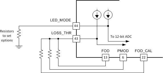 Figure 5. Pin 43 LOSS_THR and Pin 44 LED_MODE Connections
8.3.7 LED Modes
The bq500414Q can directly drive three LED outputs (pin 7, pin 8, and pin 9) through a simple current limit resistor (typically 470-Ω), based on the mode selected. The three current limit resistors can be individually adjusted to tune or match the brightness of the LEDs. Do not exceed the maximum output current rating of the device.
The selection resistor, connected between pin 44 and GND, selects one of the desired LED indication schemes presented in Table 1.
Table 1. LED Modes
| LED CONTROL OPTION |
LED SELECTION RESISTOR |
DESCRIPTION | LED | OPERATIONAL STATES | ||||
|---|---|---|---|---|---|---|---|---|
| STANDBY | POWER TRANSFER |
CHARGE COMPLETE |
FAULT | FOD Warning | ||||
| X | < 36.5 kΩ | Reserved, do not use | LED1, green | - | - | - | - | - |
| LED2, red | ||||||||
| LED3, amber | ||||||||
| 1 | 42.2 kΩ | Choice number 1 | LED1, green | Off | Blink slow(1) | On | Off | Off |
| LED2, red | Off | Off | Off | On | Blink fast(2) | |||
| LED3, amber | - | - | - | - | - | |||
| 2 | 48.7 kΩ | Choice number 2 | LED1, green | On | Blink slow(1) | On | Off | Off |
| LED2, red | On | Off | Off | On | Blink fast(2) | |||
| LED3, amber | - | - | - | - | - | |||
| 3(3) | 56.2 kΩ | Choice number 3 | LED1, green | Off | On | Off | Blink fast(2) | On |
| LED2, red | - | - | - | - | - | |||
| LED3, amber | - | - | - | - | - | |||
| 4 | 64.9 kΩ | Choice number 4 | LED1, green | Off | On | Off | Off | Off |
| LED2, red | Off | Off | Off | On | Blink fast(2) | |||
| LED3, amber | - | - | - | - | - | |||
| 5 | 75 kΩ | Choice number 5 | LED1, green | Off | Off | On | Off | Off |
| LED2, red | Off | On | Off | Off | On | |||
| LED3, amber | Off | Off | Off | Blink slow(1) | Off | |||
| 6 | 86.6 kΩ | Choice number 6 | LED1, green | Off | Blink slow(1) | On | Off | Off |
| LED2, red | Off | Off | Off | On | Blink fast(2) | |||
| LED3, amber | Off | Off | Off | Off | Off | |||
| 7 | 100 kΩ | Choice number 7 | LED1, green | Off | Blink slow(1) | Off | Off | Off |
| LED2, red | Off | Off | On | Off | Off | |||
| LED3, amber | Off | Off | Off | On | Blink fast(2) | |||
8.3.8 Foreign Object Detection (FOD) and Parasitic Metal Object Detect (PMOD) Calibration
The bq500414Q supports improved FOD (WPC v1.1) and enhanced PMOD (WPC v1.0) features. Continuously monitoring input power, known losses, and the value of power reported by the Rx device being charged, the bq500414Q can estimate how much power is unaccounted for and presumed lost due to metal objects placed in the wireless power transfer path. If this unexpected loss exceeds the threshold set by the FOD or PMOD resistors, a fault is indicated and power transfer is halted. Whether the FOD or the PMOD algorithm is used is determined by the ID packet of the receiver being charged. The ultimate goal of the FOD feature is to protect misplaced metal objects from becoming hot. Reducing the loss threshold and making the system too sensitive will lead to false trips and a bad user experience. Find the balance which best suits the application. If the application requires disabling one function or the other (or both), it is possible by leaving the respective FOD/PMOD pin open. For example, to selectively disable the PMOD function, PMOD (pin 6) should be left open.
NOTE
Disabling FOD results in a Tx solution that is not WPC 1.1 Compliant
Resistors of 1% tolerance should be used for a reliable selection of the desired threshold. The FOD and PMOD resistors (pin 13 and pin 6) program the permitted power loss for the FOD and PMOD algorithms respectively. The FOD_CAL resistor (pin 22), can be used to compensate for any load dependent effect on the power loss. Using a calibrated FOD reference receiver with no foreign objects present, the FOD_CAL resistor should be selected such that the calculated loss across the load range is substantially constant (within ~100-mW). After correcting for the load dependence, the FOD and PMOD thresholds should be re-set above the resulting average by approximately 400-mW in order for the transmitter to satisfy the WPC requirements on tolerated heating.
Contact Texas Instruments for the Tx Tuning Tool to set appropriate FOD, PMOD, and FOD_CAL resistor values for your design.
Table 2. Option Select Bins
| BIN NUMBER | RESISTANCE (kΩ) | LOSS THRESHOLD (mW) |
|---|---|---|
| 0 | < 36.5 | 250 |
| 1 | 42.2 | 300 |
| 2 | 48.7 | 350 |
| 3 | 56.2 | 400 |
| 4 | 64.9 | 450 |
| 5 | 75.0 | 500 |
| 6 | 86.6 | 550 |
| 7 | 100 | 600 |
| 8 | 115 | 650 |
| 9 | 133 | 700 |
| 10 | 154 | 750 |
| 11 | 178 | 800 |
| 12 | 205 | 850 |
| 13 | > 237 | Feature Disabled |
8.3.9 Shut Down via External Thermal Sensor or Trigger
Typical applications of the bq500414Q do not require additional thermal protection. This shutdown feature is provided for enhanced applications and is not limited to thermal shutdown. The key parameter is the 1.0-V threshold on pin 2 T_SENSE. Voltage below 1.0-V on pin 2 causes the device to shut down.
The application of thermal monitoring via a Negative Temperature Coefficient (NTC) sensor, for example, is straightforward. The NTC forms the lower leg of a temperature dependant voltage divider. The NTC leads are connected to the bq500414Q device, pin 2 and GND. The threshold on pin 2 is set to 1.0 V, below which the system shuts down and a fault is indicated (depending on LED mode chosen).
To implement this feature follow these steps:
- Consult the NTC datasheet and find the resistence vs temperature curve.
- Determine the actual temperature where the NTC will be placed by using a thermal probe.
- Read the NTC resistance at that temperature in the NTC datasheet, that is R_NTC.
- Use the following formula to determine the upper leg resistor (R_Setpoint):

The system restores normal operation after approximately five minutes or if the receiver is removed. If the feature is not used, this pin must be pulled high.
NOTE
Pin 2 T_SENSE must always be terminated, otherwise erratic behavior may occur.
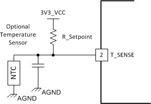 Figure 6. Negative Temperature Coefficient (NTC) Application
8.3.10 Fault Handling and Indication
The following is a table of End Power Transfer (EPT) packet responses, fault conditions, and the duration how long the condition lasts until a retry in attempted. The LED mode selected determines how the LED indicates the condition or fault.
Table 3. Fault Handling and Indication
| CONDITION | DURATION (2)
(BEFORE RETRY) |
HANDLING |
|---|---|---|
| EPT-00 | Immediate(1) | Unknown |
| EPT-01 | 5 seconds | Charge complete |
| EPT-02 | Infinite | Internal fault |
| EPT-03 | 5 minutes | Over temperature |
| EPT-04 | Immediate(1) | Over voltage |
| EPT-05 | Immediate(1) | Over current |
| EPT-06 | Infinite | Battery failure |
| EPT-07 | Not applicable | Reconfiguration |
| EPT-08 | Immediate(1) | No response |
| OVP (over voltage) | Immediate(1) | |
| OC (over current) | 1 minute | |
| NTC (external sensor) | 5 minutes | |
| PMOD/FOD warning | 12 seconds | 10 seconds LED only, 2 seconds LED + buzzer |
| PMOD/FOD | 5 minutes |
8.3.11 Power Transfer Start Signal
The bq500414Q features two signal outputs to indicate that power transfer has begun. Pin 23 BUZ_AC outputs a 400-ms duration, 4-kHz square wave for driving low cost AC type ceramic buzzers. Pin 24 BUZ_DC outputs logic high, also for 400-ms, which is suitable for DC type buzzers with built-in tone generators, or as a trigger for any type of customized indication scheme. Do not exceed 4-mA loading from either of these pins which is more than adequate for small signaling and actuation. If not used, these pins should be left open.
8.3.12 Power-On Reset
The bq500414Q has an integrated Power-On Reset (POR) circuit which monitors the supply voltage and handles the correct device startup sequence. Additional supply voltage supervisor or reset circuits are not needed.
8.3.13 External Reset, RESET Pin
The bq500414Q can be forced into a reset state by an external circuit connected to the RESET pin. A logic low voltage on this pin holds the device in reset. For normal operation, this pin is pulled up to 3.3-V supply with a 10-kΩ pull-up resistor.
8.3.14 Trickle Charge and CS100
The WPC specification provides an End-of-Power Transfer message (EPT–01) to indicate charge complete. Upon receipt of the charge complete message, the bq500414Q will change the LED indication. The exact indication depends on the LED_MODE chosen.
In some battery charging applications there is a benefit to continue the charging process in trickle-charge mode to top off the battery. There are several information packets in the WPC specification related to the levels of battery charge (Charge Status). The bq500414Q uses these commands to enable top-off charging. The bq500414Q changes the LED indication to reflect charge complete when a Charge Status message is 100% received, but unlike the response to an EPT, it will not halt power transfer while the LED indicates charge complete. The mobile device can use a CS100 packet to enable trickle charge mode.
If the reported charge status drops below 90%, normal charging indication will be resumed.
8.3.14.1 Over-Current Protection
The bq500414Q has an integrated current protection feature which monitors the input current reported by the current sense resistor and amplifier. If the input current exceeds a predetermined threshold, a fault is indicated and power transfer is halted for one minute.
If this feature is desired, the sense resistor and amplifier are required. If this feature is not desired, and WPC v1.1 compliant (FOD) is not required, the I_SENSE input pin to the bq500414Q (pin 42) should be grounded.
NOTE
Always terminate the I_SENSE pin (pin 42), either with the output of a current monitor circuit or by connecting to ground.
8.3.15 Over-Voltage Protection
When the Rx is quickly moved from a low coupling position to a high coupling position, the rectified voltage on the Rx could get to very high before the Tx reacts to the change. Per WPC protocol, there is certain time duration between the Control Error Packages, so the Tx will not be able to react instantaneously. The bq500414Q uses a peak-detect circuit to prevent the Rx from being over-voltage.
8.4 Device Functional Modes
8.4.1 Power Transfer
Power transfer depends on coil coupling. Coupling is dependant on the distance between coils, alignment, coil dimensions, coil materials, number of turns, magnetic shielding, impedance matching, frequency, and duty cycle.
Most importantly, the receiver and transmitter coils must be aligned for best coupling and efficient power transfer. The smaller the space between the coils is, the better the coupling; however, the practical distance is set to be less than 5-mm, as defined within the WPC specification, to account for housing and interface surfaces.
Shielding is added as a backing to both the transmitter and receiver coils to direct the magnetic field to the coupled zone. Magnetic fields outside the coupled zone do not transfer power. Thus, shielding also serves to contain the fields to avoid coupling to other adjacent system components.
Regulation can be achieved by controlling any one of the coil coupling parameters. However, for WPC compatibility, the transmitter-side coils and capacitance are specified and the resonant frequency point is fixed. Power transfer is thus regulated by changing the frequency along the resonance curve from 120-kHz to 205-kHz, (that is the higher the frequency is, the lower the power). Duty cycle remains constant at 50% throughout the power band and is reduced only once 205-kHz is reached.
The WPC standard describes the dimensions, materials of the coils, and information regarding the tuning of the coils to resonance. The value of the inductor and resonant capacitor are critical to proper operation and system efficiency.
8.4.2 Communication
Communication within the WPC is from the receiver to the transmitter, where the receiver tells the transmitter to send power and how much. In order to regulate, the receiver must communicate with the transmitter whether to increase or decrease frequency. The receiver monitors the rectifier output and using Amplitude Modulation (AM), sends packets of information to the transmitter. A packet is comprised of a preamble, a header, the actual message and a checksum, as defined by the WPC standard.
The receiver sends a packet by modulating an impedance network. This AM signal reflects back as a change in the voltage amplitude on the transmitter coil. The signal is demodulated and decoded by the transmitter-side electronics and the frequency of its coil-drive output is adjusted to close the regulation loop. The bq500414Q features internal digital demodulation circuitry.
The modulated impedance network on the receiver can either be resistive or capacitive. Figure 7 shows the resistive modulation approach, where a resistor is periodically added to the load, and the resulting amplitude change in the transmitter voltage. Figure 8 shows the capacitive modulation approach, where a capacitor is periodically added to the load and the resulting amplitude change in the transmitter voltage.
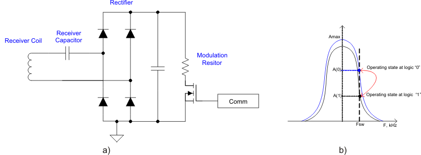 Figure 7. Receiver Resistive Modulation Circuit
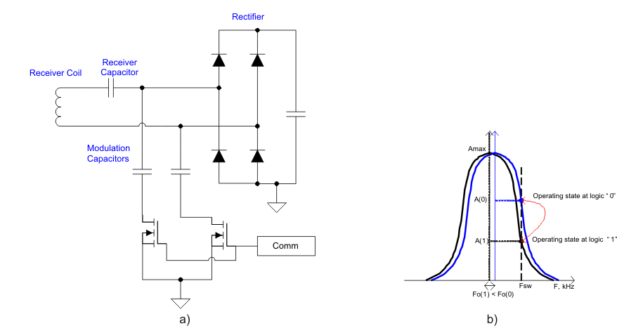 Figure 8. Receiver Capacitive Modulation Circuit
8.4.3 Power Trains
The bq500414Q drives three independent half bridges. Each half bridge drives one coil from the coil set assembly. The TPS28225 is the recommended driver device for this application. It features high-side drive capability which enables the use of N-channel MOSFETs throughout. Gate-drive supply can be derived from a primitive active voltage divider. A highly regulated supply is not required to drive MOSFET gates.
8.4.4 Signal Processing Components
The COMM signal used to control power transfer is derived from the coil voltage. Each coil has its own signal processing chain. The AC coupled coil voltage is scaled down to a manageable level and biased to a 1-V offset. Series connected diodes are provided for protection from any possible transients. The three signal processing chains are then multiplexed together via analog switches. Thus, the correct signal processing chain and COMM signal used to control power transfer is from the coil being driven.