SLUSBE4B January 2014 – June 2014
PRODUCTION DATA.
- 1 Features
- 2 Applications
- 3 Description
- 4 Simplified Diagram
- 5 Revision History
- 6 Pin Configuration and Functions
- 7 Specifications
-
8 Detailed Description
- 8.1 Overview
- 8.2 Functional Block Diagram
- 8.3
Feature Description
- 8.3.1 A6 Coil Specification
- 8.3.2 EMI Shield
- 8.3.3 I2C Interface
- 8.3.4 Active or Passive Wake-up State
- 8.3.5 Smart Key or Immobilizer Handling
- 8.3.6 Option Select Pins
- 8.3.7 LED Modes
- 8.3.8 Foreign Object Detection (FOD) and Parasitic Metal Object Detect (PMOD) CalibrationForeign Object Detection (FOD) and Parasitic Metal Object Detect (PMOD) Calibration description.
- 8.3.9 Shut Down via External Thermal Sensor or Trigger
- 8.3.10 Fault Handling and Indication
- 8.3.11 Power Transfer Start Signal
- 8.3.12 Power-On Reset
- 8.3.13 External Reset, RESET Pin
- 8.3.14 Trickle Charge and CS100
- 8.3.15 Over-Voltage Protection Over-Voltage Protection section.
- 8.4 Device Functional Modes
- 9 Applications and Implementation
- 10Power Supply Recommendations
- 11Layout
- 12Device and Documentation Support
- 13Mechanical, Packaging, and Orderable Information
Package Options
Mechanical Data (Package|Pins)
- RGZ|48
Thermal pad, mechanical data (Package|Pins)
- RGZ|48
Orderable Information
7 Specifications
7.1 Absolute Maximum Ratings(1)
over operating free-air temperature range (unless otherwise noted)| MIN | MAX | UNIT | |
|---|---|---|---|
| Voltage applied at V33D to DGND | –0.3 | 3.6 | V |
| Voltage applied at V33A to AGND | –0.3 | 3.6 | |
| Voltage applied to any pin(2) | –0.3 | 3.6 |
(1) Stresses beyond those listed under absolute maximum ratings may cause permanent damage to the device. These are stress ratings only and functional operation of the device at these or any other conditions beyond those indicated under recommended operating conditions is not implied. Exposure to absolute-maximum-rated conditions for extended periods may affect device reliability.
(2) All voltages referenced to GND.
7.2 Handling Ratings
| MIN | MAX | UNIT | ||
|---|---|---|---|---|
| Tstg | Storage temperature range | –40 | 150 | °C |
| V(ESD)(1) | Human-Body Model (HBM)(2) | 2 | 2 | kV |
| Charged-Device Model (CDM)(3) | 750 | 750 | kV |
(1) Electrostatic discharge (ESD) to measure device sensitivity and immunity to damage caused by assembly line electrostatic discharges in to the device.
(2) Level listed above is the passing level per ANSI, ESDA, and JEDEC JS-001. JEDEC document JEP155 states that 500-V HBM allows safe manufacturing with a standard ESD control process.
7.3 Recommended Operating Conditions
over operating free-air temperature range (unless otherwise noted)| MIN | NOM | MAX | UNIT | ||
|---|---|---|---|---|---|
| V | Supply voltage during operation, V33D, V33A | 3.0 | 3.3 | 3.6 | V |
| TA | Operating free-air temperature range | –40 | 85 | °C | |
| TJ | Junction temperature | 85 |
7.4 Thermal Information
| THERMAL METRIC(1) | bq500414Q | UNIT | |
|---|---|---|---|
| RGZ 48 PINS |
|||
| RθJA | Junction-to-ambient thermal resistance | 27.1 | °C/W |
| RθJC(top) | Junction-to-case (top) thermal resistance | 12.9 | |
| RθJB | Junction-to-board thermal resistance | 4.3 | |
| ψJT | Junction-to-top characterization parameter | 0.2 | |
| ψJB | Junction-to-board characterization parameter | 4.3 | |
| RθJC(bot) | Junction-to-case (bottom) thermal resistance | 0.6 | |
(1) For more information about traditional and new thermal metrics, see the IC Package Thermal Metrics application report, SPRA953.
7.5 Electrical Characteristics
over operating free-air temperature range (unless otherwise noted)| PARAMETER | TEST CONDITIONS | MIN | NOM | MAX | UNIT | ||
|---|---|---|---|---|---|---|---|
| SUPPLY CURRENT | |||||||
| IV33A | Supply current | V33A = 3.3 V | 8 | 15 | mA | ||
| IV33D | V33D = 3.3 V | 44 | 55 | ||||
| ITotal | V33D = V33A = 3.3 V | 52 | 60 | ||||
| INTERNAL REGULATOR CONTROLLER INPUTS/OUTPUTS | |||||||
| V33 | 3.3-V linear regulator | Emitter of NPN transistor | 3.25 | 3.3 | 3.6 | V | |
| V33FB | 3.3-V linear regulator feedback | 4 | 4.6 | ||||
| IV33FB | Series pass base drive | VIN = 12 V; current into V33FB pin | 10 | mA | |||
| Beta | Series NPN pass device | 40 | |||||
| EXTERNALLY SUPPLIED 3.3 V POWER | |||||||
| V33D | Digital 3.3-V power | TA = 25°C | 3 | 3.6 | V | ||
| V33A | Analog 3.3-V power | TA = 25°C | 3 | 3.6 | |||
| V33Slew | 3.3-V slew rate | 3.3-V slew rate between 2.3 V and 2.9 V, V33A = V33D |
0.25 | V/ms | |||
| DIGITAL DEMODULATION INPUTS: COMM_A+, COMM_A-, COMM_B+, COMM_B- | |||||||
| VCM | Common mode voltage each pin | –0.15 | 1.631 | V | |||
| COMM+, COMM- | Modulation voltage digital resolution | 1 | mV | ||||
| REA | Input Impedance | Ground reference | 0.5 | 1.5 | 3 | MΩ | |
| IOFFSET | Input offset current | 1-kΩ source impedance | –5 | 5 | µA | ||
| ANALOG INPUTS: V_IN, V_SENSE, I_SENSE, T_SENSE, LED_MODE, LOSS_THR | |||||||
| VADC_OPEN | Voltage indicating open pin | LED_MODE, LOSS_THR open | 2.37 | V | |||
| VADC_SHORT | Voltage indicating pin shorted to GND | LED_MODE, LOSS_THR shorted to ground | 0.36 | ||||
| VADC_RANGE | Measurement range for voltage monitoring | ALL ANALOG INPUTS | 0 | 2.5 | |||
| INL | ADC integral nonlinearity | –2.5 | 2.5 | mV | |||
| Ilkg | Input leakage current | 3 V applied to pin | 100 | nA | |||
| RIN | Input impedance | Ground reference | 8 | MΩ | |||
| CIN | Input capacitance | 10 | pF | ||||
| DIGITAL INPUTS/OUTPUTS | |||||||
| VOL | Low-level output voltage | IOL = 6 mA , V33D = 3 V | DGND1 + 0.25 | V | |||
| VOH | High-level output voltage | IOH = –6 mA , V33D = 3 V | V33D – 0.6 V |
||||
| VIH | High-level input voltage | V33D = 3 V | 2.1 | 3.6 | |||
| VIL | Low-level input voltage | V33D = 3.5 V | 1.4 | ||||
| IOH(MAX) | Output high source current | 4 | mA | ||||
| IOL(MAX) | Output low sink current | 4 | |||||
| SYSTEM PERFORMANCE | |||||||
| VRESET | Voltage where device comes out of reset | V33D pin | 2.4 | V | |||
| tRESET | Pulse width needed for reset | RESET pin | 2 | µs | |||
| fSW | Switching Frequency | 120 | 205 | kHz | |||
| tdetect | Time to detect presence of device requesting power | 0.5 | s | ||||
7.6 Typical Characteristics
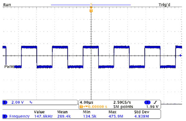 Figure 1. Typical PWM Signal
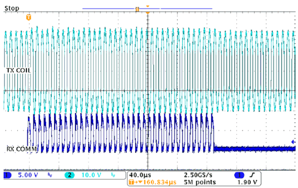 Figure 3. Tx Coil and Rx Communication Signals
with Rx No Load
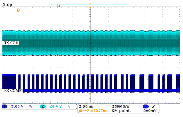 Figure 2. Typical Tx Coil and Rx Communication Signals
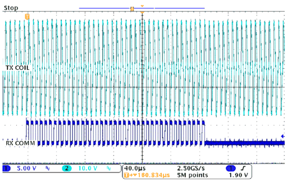 Figure 4. Tx Coil and Rx Communication Signals
with Rx 5W Load