SLUSBE4B January 2014 – June 2014
PRODUCTION DATA.
- 1 Features
- 2 Applications
- 3 Description
- 4 Simplified Diagram
- 5 Revision History
- 6 Pin Configuration and Functions
- 7 Specifications
-
8 Detailed Description
- 8.1 Overview
- 8.2 Functional Block Diagram
- 8.3
Feature Description
- 8.3.1 A6 Coil Specification
- 8.3.2 EMI Shield
- 8.3.3 I2C Interface
- 8.3.4 Active or Passive Wake-up State
- 8.3.5 Smart Key or Immobilizer Handling
- 8.3.6 Option Select Pins
- 8.3.7 LED Modes
- 8.3.8 Foreign Object Detection (FOD) and Parasitic Metal Object Detect (PMOD) CalibrationForeign Object Detection (FOD) and Parasitic Metal Object Detect (PMOD) Calibration description.
- 8.3.9 Shut Down via External Thermal Sensor or Trigger
- 8.3.10 Fault Handling and Indication
- 8.3.11 Power Transfer Start Signal
- 8.3.12 Power-On Reset
- 8.3.13 External Reset, RESET Pin
- 8.3.14 Trickle Charge and CS100
- 8.3.15 Over-Voltage Protection Over-Voltage Protection section.
- 8.4 Device Functional Modes
- 9 Applications and Implementation
- 10Power Supply Recommendations
- 11Layout
- 12Device and Documentation Support
- 13Mechanical, Packaging, and Orderable Information
Package Options
Mechanical Data (Package|Pins)
- RGZ|48
Thermal pad, mechanical data (Package|Pins)
- RGZ|48
Orderable Information
11 Layout
11.1 Layout Guidelines
Careful PCB layout practice is critical to proper system operation. There are many references on proper PCB layout techniques. A few good tips are as follows:
The Tx layout requires a 4-layer PCB layout for best ground plane technique. A 2-layer PCB layout can be achieved though not as easily. Ideally, the approach to the layer stack-up has been:
- Layer 1 component placement and as much ground plane as possible
- Layer 2 clean ground
- Layer 3 finish routing
- Layer 4 clean ground
Thus, the circuitry is virtually sandwiched between grounds. This minimizes EMI noise emissions and also provides a noise free voltage reference plane for device operation.
Keep as much copper as possible. Make sure the bq500414Q GND pins and the EPAD GND power pad have a continuous flood connection to the ground plane. The power pad should also be stitched to the ground plane, which also acts as a heat sink for the bq500414Q. A good GND reference is necessary for proper bq500414Q operation, such as analog-digital conversion, clock stability and best overall EMI performance.
Separate the analog ground plane from the power ground plane and use only ONE tie point to connect grounds. Having several tie points defeats the purpose of separating the grounds.
The COMM return signal from the resonant tank should be routed as a differential pair. This is intended to reduce stray noise induction. The frequencies of concern warrant low-noise analog signaling techniques, such as differential routing and shielding, but the COMM signal lines do not need to be impedance matched.
The DC-DC buck regulator used from the 12-V input supplies the bq500414Q with 3.3-V. Typically a single-chip controller solution with integrated power FET and synchronous rectifier or outboard diode is used. Pull in the buck inductor and power loop as close as possible to create a tight loop. Likewise, the power-train, full-bridge components should be pulled together as tight as possible. See the bq500414Q EVM for an example of a good layout technique.
11.2 Layout Example
A DC-DC buck regulator is used to step down the system voltage to the 3.3-V supply to the bq500414Q. The system voltage could be 12-V, or 6-V – 16-V depending on where the buck regulator input is. With such a step-down ratio, switching duty-cycle will be low and the regulator will be mostly freewheeling. Therefore, place the freewheeling diode current loop as close to the switching regulator as possible (loop in red). Place the buck inductor and power loop as close to that as possible (loop in blue).
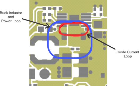 Figure 14. DC-DC Buck Regulator Layout
Make sure the bypass capacitors intended for the bq500414Q 3.3-V supply are actually bypassing these supply pins (pin 33 V33D and pin 34 V33A) to solid ground plane. This means they need to be placed as close to the device as possible and the traces must be as wide as possible.
 Figure 15. Bypass Capacitors Layout
Make sure the bq500414Q has a continuous flood connection to the ground plane.
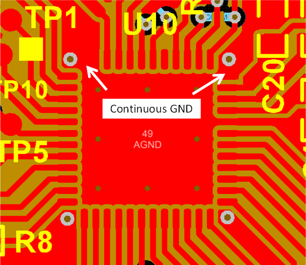 Figure 16. Continuous GND Layout
Proper current sensing layout technique is very important, as it directly affects the FOD and PMOD performance. When sampling the very low voltages generated across a current sense resistor, be sure to use the so called, "Four-wire" or "Kelvin-connection" technique. This is important to avoid introducing false voltage drops from adjacent pads and copper power routes. It is common power supply layout technique.
In the below screen shot of a Texas Instruments PCB layout, the current sense resistor is R64. Notice the R18 and R15 sensing resisters are connected to the pads of R64 so there is no measurement error introduced by copper conduction losses or copper resistance temperature dependency.
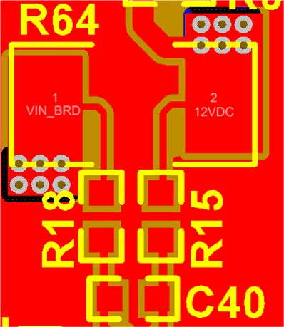 Figure 17. Current Sensing Layout
COMM+/COMM– sense lines should be run as a balanced or differential pair. The WPC packet information runs at 2-kHz, which is essential audio frequency content and this balancing reduces noise pickup from the surrounding switching power electronics. There is no need to tune or impedance-match these lines as would be the case in RF signaling.
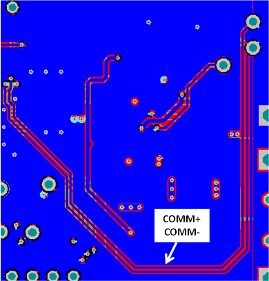 Figure 18. Balanced COMM Lines Layout