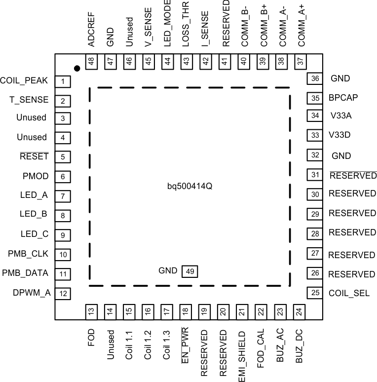
| COIL_PEAK |
1 |
I |
Input from peak detect circuit |
| T_SENSE |
2 |
I |
Sensor input. Device shuts down when below 1 V. If not used, keep above 1 V by simply connecting to 3.3-V supply |
| Unused |
3 |
I |
This pin can be either connected to GND or left open. Connecting to GND can improve layout grounding |
| Unused |
4 |
I |
This pin can be either connected to GND or left open. Connecting to GND can improve layout grounding |
| RESET |
5 |
I |
Device reset. Use 10-kΩ to 100-kΩ pull-up resistor to 3.3-V supply |
| PMOD |
6 |
O |
Select for PMOD threshold |
| LED_A |
7 |
O |
Connect to a LED via 470-Ω resistor for status indication. Typically GREEN |
| LED_B |
8 |
O |
Connect to a LED via 470-Ω resistor for status indication. Typically RED |
| LED_C |
9 |
O |
Connect to a LED via 470-Ω resistor for status indication. Typically YELLOW |
| PMB_CLK |
10 |
I/O |
10-kΩ pull-up resistor to 3.3-V supply. I2C Clock |
| PMB_DATA |
11 |
I/O |
10-kΩ pull-up resistor to 3.3-V supply. I2C Data |
| DPWM_A |
12 |
O |
PWM Output to half bridge driver. Switching dead times must be externally generated |
| FOD |
13 |
O |
Select for FOD threshold |
| Unused |
14 |
O |
Reserved, leave this pin open |
| COIL 1.1 |
15 |
O |
Enables the first coil drive train and COMM signal selector |
| COIL 1.2 |
16 |
O |
Enables the second coil drive train and COMM signal selector |
| COIL 1.3 |
17 |
O |
Enables the third coil drive train and COMM signal selector |
| EN_PWR |
18 |
I/O |
Enable signal to the front end converter. Select the active or passive wake-up state |
| RESERVED |
19 |
O |
Reserved, leave this pin open |
| RESERVED |
20 |
I |
Reserved, connect to GND |
| EMI_SHIELD |
21 |
I |
Connect to 3.3-V supply to indicate EMI shield is in use. If not, connect this pin to GND |
| FOD_CAL |
22 |
O |
FOD Calibration |
| BUZ_AC |
23 |
O |
AC buzzer output. A 400-ms, 4-kHz AC pulse train when charging begins |
| BUZ_DC |
24 |
O |
DC buzzer output. A 400-ms DC pulse when charging begins. This could also be connected to an LED via 470-Ω resistor |
| COIL_SEL |
25 |
I |
Coil type select. Connect to GND for A6 typle Tx |
| RESERVED |
26 |
I/O |
Reserved, connect to GND |
| RESERVED |
27 |
I/O |
Reserved, leave this pin open |
| RESERVED |
28 |
I/O |
Reserved, leave this pin open |
| RESERVED |
29 |
I/O |
Reserved, leave this pin open |
| RESERVED |
30 |
I/O |
Reserved, leave this pin open |
| RESERVED |
31 |
I/O |
Reserved, connect 10-kΩ pull-down resistor to GND. Do not leave open |
| GND |
32 |
— |
GND |
| V33D |
33 |
— |
Digital Core 3.3-V supply. Be sure to decouple with bypass capacitors as close to the part as possible |
| V33A |
34 |
— |
Analog 3.3-V supply. This pin can be derived from V33D supply, decouple with 22-Ω resistor and additional bypass capacitors |
| BPCAP |
35 |
— |
Bypass capacitor for internal 1.8-V core regulator. Connect bypass capacitors to GND and to 3.3-V |
| GND |
36 |
— |
GND |
| COMM_A+ |
37 |
I |
Digital demodulation noninverting input A, connect parallel to input B+ |
| COMM_A- |
38 |
I |
Digital demodulation inverting input A, connect parallel to input B- |
| COMM_B+ |
39 |
I |
Digital demodulation noninverting input B, connect parallel to input A+ |
| COMM_B- |
40 |
I |
Digital demodulation inverting input B, connect parallel to input A- |
| RESERVED |
41 |
I |
Reserved, leave this pin open |
| I_SENSE |
42 |
I |
Transmitter input current, used for parasitic loss calculations. Use 40-mΩ sense resistor and A = 50 gain current sense amp |
| LOSS_THR |
43 |
I |
Input to program FOD/PMOD thresholds and FOD_CAL correction |
| LED_MODE |
44 |
I |
LED Mode Select |
| V_SENSE |
45 |
I |
Transmitter power train input voltage, used for FOD and Loss calculations. |
| Unused |
46 |
I |
This pin can be either connected to GND or left open. Connecting to GND can improve layout grounding |
| GND |
47 |
— |
GND |
| ADCREF |
48 |
I |
External reference voltage input. Connect this input to GND. |
| EPAD |
49 |
— |
Flood with copper GND plane and stitch vias to PCB internal GND plane |