SBAS422B July 2007 – January 2018 DAC8881
PRODUCTION DATA.
- 1 Features
- 2 Applications
- 3 Description
- 4 Revision History
- 5 Pin Configuration and Functions
- 6 Specifications
-
7 Detailed Description
- 7.1 Overview
- 7.2 Functional Block Diagram
- 7.3 Feature Description
- 7.4 Device Functional Modes
- 8 Application and Implementation
- 9 Power Supply Recommendations
- 10Layout
- 11Device and Documentation Support
Package Options
Mechanical Data (Package|Pins)
- RGE|24
Thermal pad, mechanical data (Package|Pins)
- RGE|24
Orderable Information
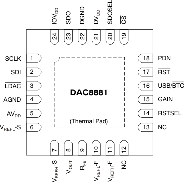
5 Pin Configuration and Functions
RGE Package1
QFN-24
(Top View)

1. The thermal pad is internally connected to the substrate. This pad can be connected to the analog ground or left floating. Keep the thermal pad separate from the digital ground, if possible.
Pin Functions
| PIN | I/O | DESCRIPTION | |
|---|---|---|---|
| NO. | NAME | ||
| 1 | SCLK | I | SPI bus serial clock input |
| 2 | SDI | I | SPI bus serial data input |
| 3 | LDAC | I | Load DAC latch control input (active low). When LDAC is low, the DAC latch is transparent, and the contents of the input register are transferred to the DAC latch. The DAC output changes to the corresponding level simultaneously when the DAC latch is updated. |
| 4 | AGND | I | Analog ground |
| 5 | AVDD | I | Analog power supply |
| 6 | VREFL-S | I | Reference low input sense |
| 7 | VREFH-S | I | Reference high input sense |
| 8 | VOUT | O | Output of output buffer |
| 9 | RFB | I | Feedback resistor connected to the inverting input of the output buffer. |
| 10 | VREFL-F | I | Reference low input force |
| 11 | VREFH-F | I | Reference high input force |
| 12 | NC | — | Do not connect. |
| 13 | NC | — | Do not connect. |
| 14 | RSTSEL | I | Selects the value of the output from the VOUT pin after power-on or hardware reset. If RSTSEL = IOVDD, then register data = 8000h. If RSTSEL = DGND, then register data = 0000h. |
| 15 | GAIN | I | Buffer gain setting. Gain = 1 when the pin is connected to DGND; Gain = 2 when the pin is connected to IOVDD. |
| 16 | USB/BTC | I | Input data format selection. Input data are straight binary format when the pin is connected to IOVDD, and in two’s complement format when the pin is connected to DGND. |
| 17 | RST | I | Reset input (active low). Logic low on this pin causes the device to perform a reset. |
| 18 | PDN | I | Power-down input (active high). Logic high on this pin forces the device into power-down status. In power-down, the VOUT pin connects to AGND through 10kΩ resistor. |
| 19 | CS | I | SPI bus chip select input (active low). Data bits are not clocked into the serial shift register unless CS is low. When CS is high, SDO is in high-impedance status. |
| 20 | SDOSEL | I | SPI serial data output selection. When SDOSEL is tied to IOVDD, the contents of the existing input register are shifted out from the SDO pin; this is Stand-Alone mode. When SDOSEL is tied to DGND, the contents in the SPI input shift register are shifted out from the SDO pin; this is Daisy-Chain mode for daisy chaining communication. |
| 21 | DVDD | I | Digital power supply (connect to AVDD, pin 5) |
| 22 | DGND | I | Digital ground |
| 23 | SDO | O | SPI bus serial data output. Refer to the Timing Diagrams for further detail. |
| 24 | IOVDD | I | Interface power. Connect to +1.8V for 1.8V logic, +3V for 3V logic, and to +5V for 5V logic. |