SBAS422B July 2007 – January 2018 DAC8881
PRODUCTION DATA.
- 1 Features
- 2 Applications
- 3 Description
- 4 Revision History
- 5 Pin Configuration and Functions
- 6 Specifications
-
7 Detailed Description
- 7.1 Overview
- 7.2 Functional Block Diagram
- 7.3 Feature Description
- 7.4 Device Functional Modes
- 8 Application and Implementation
- 9 Power Supply Recommendations
- 10Layout
- 11Device and Documentation Support
Package Options
Mechanical Data (Package|Pins)
- RGE|24
Thermal pad, mechanical data (Package|Pins)
- RGE|24
Orderable Information
6.9 TYpical Characteristics: VDD = +2.7 V
At TA = +25°C, VREFH = +2.5 V, VREFL = 0 V, and Gain = 1X Mode, unless otherwise noted.
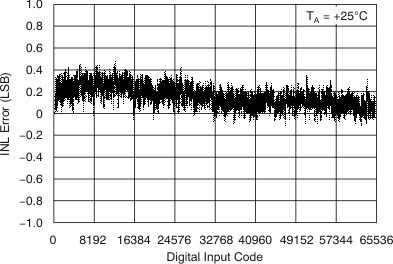 Figure 44. Linearity Error vs Digital Input Code
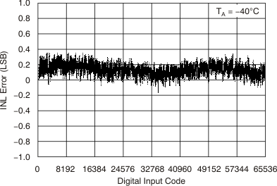 Figure 46. Linearity Error vs Digital Input Code
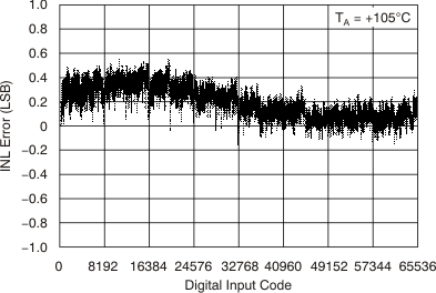 Figure 48. Linearity Error vs Digital Input Code
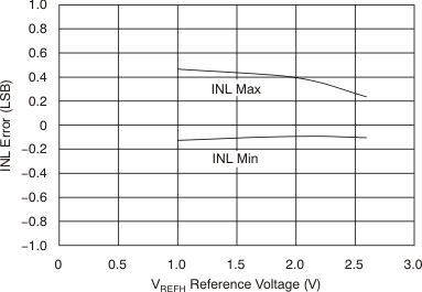 Figure 50. Linearity Error vs
 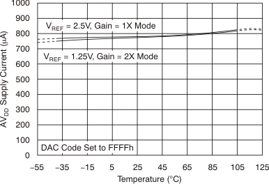 Figure 52. AVDD Supply Current vs Temperature
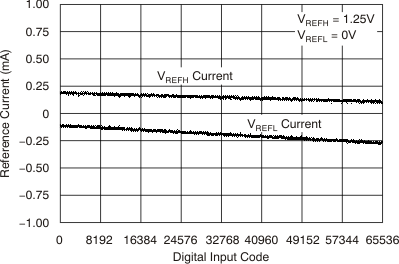 Figure 54. Reference Current vs Digital Input Code
(Gain = 2X Mode)
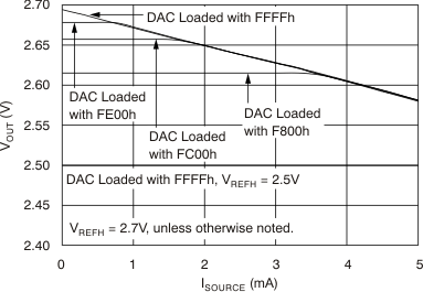 Figure 56. Output Voltage vs Drive Current Capability
(Operation Near AVDD Rail)
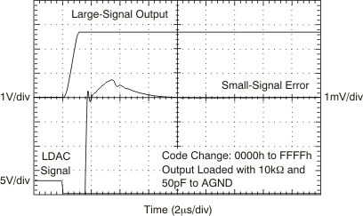 Figure 58. Large Signal Settling Time
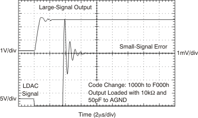 Figure 60. Large Signal Settling Time
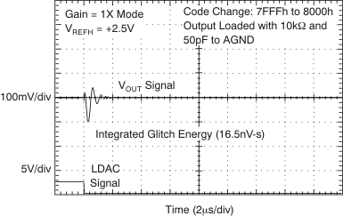 Figure 62. Major Carry Glitch
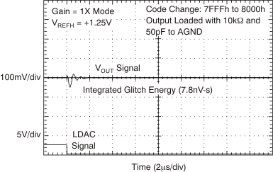 Figure 64. Major Carry Glitch
 Figure 45. Differential Linearity Error vs Digital Input Code
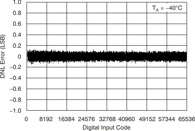 Figure 47. Differential Linearity Error vs Digital Input Code
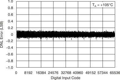 Figure 49. Differential Linearity Error vs Digital Input Code
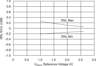 Figure 51. Differential Linearity Error vs Reference Voltage
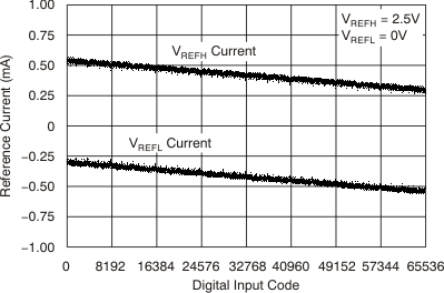 Figure 53. Reference Current vs Digital Input Code
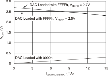 Figure 55. Output Voltage vs Drive Current Capability
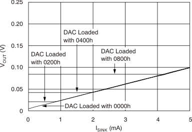 Figure 57. Output Voltage vs Drive Current Capability
 (Operation Near AGND Rail)
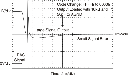 Figure 59. Large Signal Settling Time
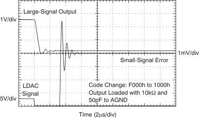 Figure 61. Large Signal Settling Time
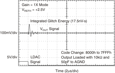 Figure 63. Major Carry Glitch
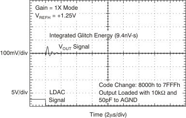 Figure 65. Major Carry Glitch