SNLS316G September 2009 – December 2015 DS90UR907Q-Q1
PRODUCTION DATA.
- 1 Features
- 2 Applications
- 3 Description
- 4 Revision History
- 5 Pin Configuration and Functions
-
6 Specifications
- 6.1 Absolute Maximum Ratings
- 6.2 ESD Ratings—JEDEC
- 6.3 ESD Ratings—IEC and ISO
- 6.4 Recommended Operating Conditions
- 6.5 Thermal Information
- 6.6 DC Electrical Characteristics
- 6.7 Recommended Timing for the Serial Control Bus
- 6.8 Switching Characteristics
- 6.9 DC and AC Serial Control Bus Characteristics
- 6.10 Typical Characteristics
-
7 Detailed Description
- 7.1 Overview
- 7.2 Functional Block Diagram
- 7.3 Feature Description
- 7.4 Device Functional Modes
- 7.5 Programming
- 8 Application and Implementation
- 9 Power Supply Recommendations
- 10Layout
- 11Device and Documentation Support
- 12Mechanical, Packaging, and Orderable Information
Package Options
Mechanical Data (Package|Pins)
- NJK|36
Thermal pad, mechanical data (Package|Pins)
Orderable Information
10 Layout
10.1 Layout Guidelines
10.1.1 PCB Layout and Power System Considerations
Design the circuit board layout and stack-up for the LVDS devices to provide low-noise power feed to the device. Good layout practice will also separate high-frequency or high-level inputs and outputs to minimize unwanted stray noise pickup, feedback, and interference. Power system performance may be greatly improved by using thin dielectrics (2 to 4 mils) for power / ground sandwiches. This arrangement provides plane capacitance for the PCB power system with low-inductance parasitics, which has proven especially effective at high frequencies, and makes the value and placement of external bypass capacitors less critical. The capacitors may use values in the range of 0.01 uF to 0.1 uF.
TI recommends surface mount capacitors due to their smaller parasitics. When using multiple capacitors per supply pin, place the smaller value closer to the pin. TI recommends a large bulk capacitor at the point of power entry. This is typically in the 50-uF to 100-uF range and will smooth low-frequency switching noise. TI recommends connecting power and ground pins directly to the power and ground planes with bypass capacitors connected to the plane with the via on both ends of the capacitor. Connecting power or ground pins to an external bypass capacitor will increase the inductance of the path.
TI recommends a small body size X7R chip capacitor, such as the 0603, for external bypass. The X7R chip capacitor's small body size reduces the parasitic inductance of the capacitor. The user must pay attention to the resonance frequency of these external bypass capacitors, usually in the range of 20 to 30 MHz. To provide effective bypassing, use multiple capacitors to achieve low impedance between the supply rails over the frequency of interest. At high frequency, it is also a common practice to use two vias from power and ground pins to the planes, reducing the impedance at high frequency.
Some devices provide separate power and ground pins for different portions of the circuit. This is done to isolate switching noise effects between different sections of the circuit. Separate planes on the PCB are typically not required. The table typically provides guidance on which circuit blocks are connected to which power pin pairs. In some cases, an external filter many be used to provide clean power to sensitive circuits such as PLLs.
Use at least a four layer board with a power and ground plane. Place LVCMOS signals away from the LVDS lines to prevent coupling from the LVCMOS lines to the LVDS lines. Closely-coupled differential lines of 100 Ω are typically recommended for LVDS interconnect. The closely coupled lines help to ensure that coupled noise will appear as common-mode and thus is rejected by the receivers. The tightly coupled lines will also radiate less.
10.1.2 LVDS Interconnect Guidelines
See SNLA008 and SNLA035 for full details.
- Use 100-Ω coupled differential pairs
- Use the S/2S/3S rule in spacings
- S = space between the pair
- 2S = space between pairs
- 3S = space to LVCMOS signal
- Minimize the number of Vias
- Use differential connectors when operating above 500-megabits per second line speed
- Maintain balance of the traces
- Minimize skew within the pair
- Terminate as close to the TX outputs and RX inputs as possible
Additional general guidance can be found in the LVDS Owner’s Manual - available in PDF format from the TI website at: www.ti.com/lvds
10.2 Layout Example
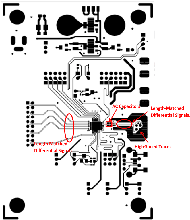
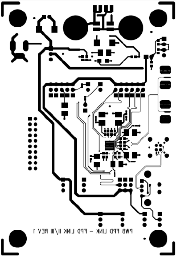
Figure 28 and Figure 29 show the PCB layout example derived from the layout design of the DS90UR907Q-Q1 Evaluation Board. The graphic and layout description are used to determine both proper routing and proper solder techniques for designing the board.
 Figure 28. Top Layer
 Figure 29. Bottom Layer