SNLS316G September 2009 – December 2015 DS90UR907Q-Q1
PRODUCTION DATA.
- 1 Features
- 2 Applications
- 3 Description
- 4 Revision History
- 5 Pin Configuration and Functions
-
6 Specifications
- 6.1 Absolute Maximum Ratings
- 6.2 ESD Ratings—JEDEC
- 6.3 ESD Ratings—IEC and ISO
- 6.4 Recommended Operating Conditions
- 6.5 Thermal Information
- 6.6 DC Electrical Characteristics
- 6.7 Recommended Timing for the Serial Control Bus
- 6.8 Switching Characteristics
- 6.9 DC and AC Serial Control Bus Characteristics
- 6.10 Typical Characteristics
-
7 Detailed Description
- 7.1 Overview
- 7.2 Functional Block Diagram
- 7.3 Feature Description
- 7.4 Device Functional Modes
- 7.5 Programming
- 8 Application and Implementation
- 9 Power Supply Recommendations
- 10Layout
- 11Device and Documentation Support
- 12Mechanical, Packaging, and Orderable Information
Package Options
Mechanical Data (Package|Pins)
- NJK|36
Thermal pad, mechanical data (Package|Pins)
Orderable Information
8 Application and Implementation
NOTE
Information in the following applications sections is not part of the TI component specification, and TI does not warrant its accuracy or completeness. TI’s customers are responsible for determining suitability of components for their purposes. Customers should validate and test their design implementation to confirm system functionality.
8.1 Application Information
The DS90UR907Q and DS90UR908Q chipset is intended for interface between a host (graphics processor) and a Display. It supports an 24-bit color depth (RGB888) and up to 1024 × 768 display formats. In a RGB888 application, 24 color bits (R[7:0], G[7:0], B[7:0]), Pixel Clock (PCLK) and three control bits (VS, HS and DE) are supported across the serial link with PCLK rates from 5 to 65 MHz. The chipset may also be used in 18-bit color applications. In this application three to six general purpose signals may also be sent from host to display.
8.1.1 Power-Up Requirements and PDB Pin
The VDD (VDDn and VDDIO) supply ramp should be faster than 1.5 ms with a monotonic rise. If slower then 1.5 ms then a capacitor on the PDB pin is needed to ensure PDB arrives after all the VDD have settled to the recommended operating voltage. When PDB pin is pulled to VDDIO, TI recommends using a 10-kΩ pullup and a 22-uF capacitor to GND to delay the PDB input signal.
8.1.2 Transmission Media
The DS90UR907Q and the companion deserializer chipset is intended to be used in a point-to-point configuration, through a PCB trace, or through twisted pair cable. The DS90UR907Q provide internal terminations providing a clean signaling environment. The interconnect for LVDS should present a differential impedance of 100 Ω. Use cables and connectors that have matched differential impedance to minimize impedance discontinuities. Shielded or unshielded cables may be used depending upon the noise environment and application requirements.
8.1.3 Alternate Color / Data Mapping
Color Mapped data pin names are provided to specify a recommended mapping for 24-bit and 18-bit Applications. When connecting to earlier generations of FPD-Link II deserializer devices, a color mapping review is recommended to ensure the correct connectivity is obtained. Table 7 provides examples for interfacing between DS90UR907Q and different deserializers.
Table 7. Alternate Color / Data Mapping
| FPD-Link | Bit Number | RGB (LSB Example) | DS90UR906Q | DS90UR124 | DS99R124Q | DS90C124 | |
|---|---|---|---|---|---|---|---|
| RxIN3 | Bit 26 | B1 | B1 | N/A | |||
| Bit 25 | B0 | B0 | |||||
| Bit 24 | G1 | G1 | |||||
| Bit 23 | G0 | G0 | |||||
| Bit 22 | R1 | R1 | |||||
| Bit 21 | R0 | R0 | |||||
| RxIN2 | Bit 20 | DE | DE | ROUT20 | TxOUT2 | ROUT20 | |
| Bit 19 | VS | VS | ROUT19 | ROUT19 | |||
| Bit 18 | HS | HS | ROUT18 | ROUT18 | |||
| Bit 17 | B7 | B7 | ROUT17 | ROUT17 | |||
| Bit 16 | B6 | B6 | ROUT16 | ROUT16 | |||
| Bit 15 | B5 | B5 | ROUT15 | ROUT15 | |||
| Bit 14 | B4 | B4 | ROUT14 | ROUT14 | |||
| RxIN1 | Bit 13 | B3 | B3 | ROUT13 | TxOUT1 | ROUT13 | |
| Bit 12 | B2 | B2 | ROUT12 | ROUT12 | |||
| Bit 11 | G7 | G7 | ROUT11 | ROUT11 | |||
| Bit 10 | G6 | G6 | ROUT10 | ROUT10 | |||
| Bit 9 | G5 | G5 | ROUT9 | ROUT9 | |||
| Bit 8 | G4 | G4 | ROUT8 | ROUT8 | |||
| Bit 7 | G3 | G3 | ROUT7 | ROUT7 | |||
| RxIN0 | Bit 6 | G2 | G2 | ROUT6 | TxOUT0 | ROUT6 | |
| Bit 5 | R7 | R7 | ROUT5 | ROUT5 | |||
| Bit 4 | R6 | R6 | ROUT4 | ROUT4 | |||
| Bit 3 | R5 | R5 | ROUT3 | ROUT3 | |||
| Bit 2 | R4 | R4 | ROUT2 | ROUT2 | |||
| Bit 1 | R3 | R3 | ROUT1 | ROUT1 | |||
| Bit 0 | R2 | R2 | ROUT0 | ROUT0 | |||
| N/A * These bits are not supported by DS90UR907Q |
N/A | ROUT23* | OS2* | ROUT23* | |||
| ROUT22* | OS1* | ROUT22* | |||||
| ROUT21* | OS0* | ROUT21* | |||||
| DS90UR907Q Settings | MAPSEL = 0 | CONFIG [1:0] = 00 | CONFIG [1:0] = 10 | CONFIG [1:0] = 11 | |||
8.2 Typical Application
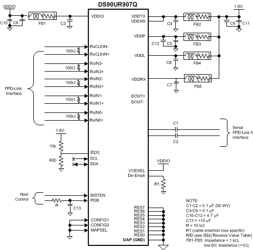
Figure 25 shows a typical application of the DS90UR907Q for a 65-MHz 24-bit Color Display Application. The LVDS inputs of the FPD-Link interface require external 100-Ω terminations. The LVDS outputs of FPD-Link II require 100-nF AC coupling capacitors to the line. The line driver includes internal termination. Bypass capacitors are placed near the power supply pins. At a minimum, four 0.1-µF capacitors and a 4.7-µF capacitor should be used for local device bypassing. System GPO (General Purpose Output) signals control the PDB and BISTEN pins. The application assumes the companion deserializer (DS90UR908Q); therefore, the configuration pins are also both tied Low. In this example the cable is long; therefore, the VODSEL pin is tied High and a De-Emphasis value is selected by the resistor R1. The interface to the host is with 1.8-V LVCMOS levels, thus the VDDIO pin is connected also to the 1.8-V rail. The Optional Serial Bus Control is not used in this example, thus the SCL, SDA and ID[x] pins are left open. A delay capacitor and resistor is placed on the PDB signal to delay the enabling of the device until power is stable. Bypass capacitors are placed near the power supply pins. Ferrite beads are placed on the power lines for effective noise suppression.
 Figure 25. Typical Connection Diagram
8.2.1 Design Requirements
Table 8 shows the input parameters for the typical design application.
Table 8. Design Parameters
| DESIGN PARAMETER | EXAMPLE VALUE |
|---|---|
| VDDIO | 1.8 V or 3.3 V |
| VDDL, VDDP, VDDHS, VDDTX, VDDRX | 1.8 V |
| AC Coupling Capacitor for DOUT± | 100 nF |
8.2.2 Detailed Design Procedure
The DOUT± outputs require 100-nF AC coupling capacitors to the line. FPD-Link data input pair required an external 100-Ω termination for standard LVDS levels. The power supply filter capacitors are placed near the power supply pins. A smaller capacitance capacitor should be located closer to the power supply pins. Adding a ferrite bead is optional. Recommend to use 1-kΩ impedance and low DC resistance such as less than 1 Ω. The VODSEL pin is tied to VDDIO for the long cable application. The De-Emph pin may connect a resistor to ground. Refer to the Table 3. The PDB and BISTEN pins are assumed controlling by a microprocessor. The PDB must be low state until all power supply voltages reach the final voltage. The CONFIG[1:0] pins are set depending on operating modes and interfacing device. See the Table 1. MAPSEL pin is set the mapping scheme. Refer to the Figure 16 and Figure 17. The SCL, SDA, and ID[x] pins are left open when these Serial Bus Control pins are unused. The RES[7:0] pins and DAP should be tied to ground.
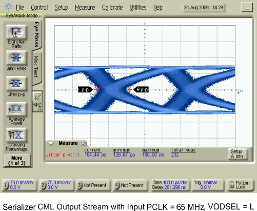
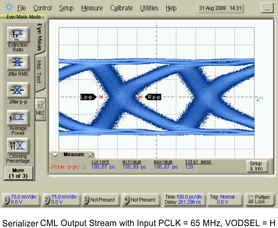
8.2.3 Application Curves

