SNVS124G November 1999 – March 2023 LM2596
PRODUCTION DATA
- 1 Features
- 2 Applications
- 3 Description
- 4 Revision History
- 5 Description (continued)
- 6 Pin Configuration and Functions
-
7 Specifications
- 7.1 Absolute Maximum Ratings
- 7.2 ESD Ratings
- 7.3 Operating Conditions
- 7.4 Thermal Information
- 7.5 Electrical Characteristics – 3.3-V Version
- 7.6 Electrical Characteristics – 5-V Version
- 7.7 Electrical Characteristics – 12-V Version
- 7.8 Electrical Characteristics – Adjustable Voltage Version
- 7.9 Electrical Characteristics – All Output Voltage Versions
- 7.10 Typical Characteristics
- 8 Detailed Description
- 9 Application and Implementation
- 10Device and Documentation Support
- 11Mechanical, Packaging, and Orderable Information
Package Options
Refer to the PDF data sheet for device specific package drawings
Mechanical Data (Package|Pins)
- NDH|5
- NEB|5
- KTT|5
Thermal pad, mechanical data (Package|Pins)
- KTT|5
Orderable Information
9.4.3 Thermal Considerations
The LM2596 is available in two packages: a 5-pin TO-220 (T) and a 5-pin surface mount TO-263 (S).
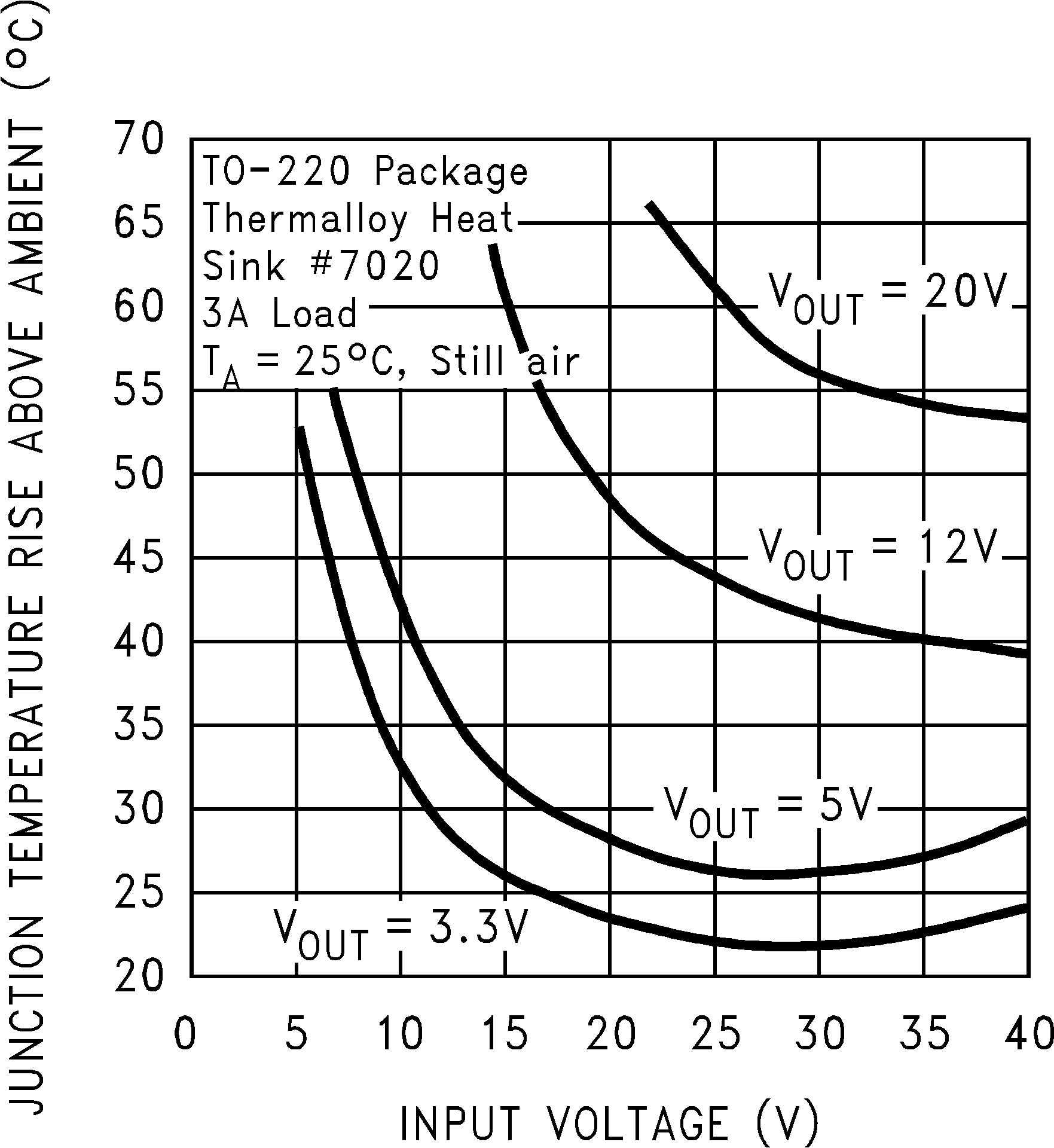
The TO-220 package requires a heat sink under most conditions. The size of the heat sink depends on the input voltage, the output voltage, the load current and the ambient temperature. Figure 9-18 shows the LM2596T junction temperature rises above ambient temperature for a 3-A load and different input and output voltages. The data for these curves was taken with the LM2596T (TO-220 package) operating as a buck switching regulator in an ambient temperature of 25°C (still air). These temperature rise numbers are all approximate and there are many factors that can affect these temperatures. Higher ambient temperatures require more heat sinking.
The TO-263 surface mount package tab is designed to be soldered to the copper on a printed-circuit board (PCB). The copper and the board are the heat sink for this package and the other heat producing components, such as the catch diode and inductor. The PCB copper area that the package is soldered to must be at least 0.4 in2, and ideally must have two or more square inches of 2-oz. (0.0028 in.) copper. Additional copper area improves the thermal characteristics, but with copper areas greater than approximately 6 in2, only small improvements in heat dissipation are realized. If further thermal improvements are required, TI recommends double-sided, multilayer PCB with large copper areas and airflow.
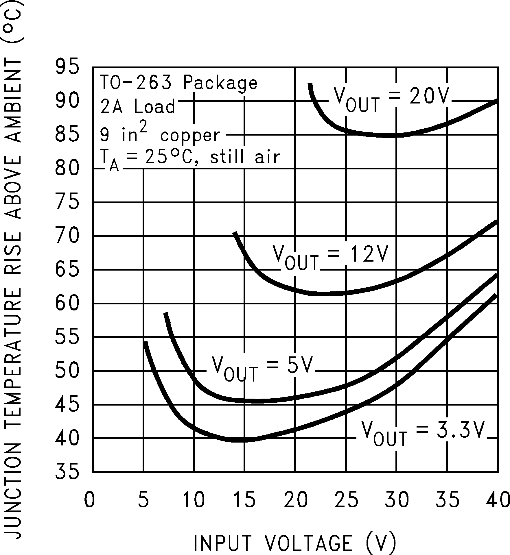
Figure 9-19 shows the LM2596S (TO-263 package) junction temperature rise above ambient temperature with a 2-A load for various input and output voltages. This data was taken with the circuit operating as a buck switching regulator with all components mounted on a PCB to simulate the junction temperature under actual operating conditions. This curve can be used for a quick check for the approximate junction temperature for various conditions, but be aware that there are many factors that can affect the junction temperature. When load currents higher than 2 A are used, double-sided or multilayer PCB with large copper areas or airflow can be required, especially for high ambient temperatures and high output voltages.
For the best thermal performance, wide copper traces and generous amounts of PCB copper must be used in the board layout. (One exception to this is the output (switch) pin, which must not have large areas of copper.) Large areas of copper provide the best transfer of heat (lower thermal resistance) to the surrounding air, and moving air lowers the thermal resistance even further.
Package thermal resistance and junction temperature rise numbers are all approximate, and there are many factors that will affect these numbers. Some of these factors include board size, shape, thickness, position, location, and even board temperature. Other factors are trace width, total printed-circuit copper area, copper thickness, single- or double-sided multilayer board, and the amount of solder on the board. The effectiveness of the PCB to dissipate heat also depends on the size, quantity, and spacing of other components on the board, as well as whether the surrounding air is still or moving. Furthermore, some of these components such as the catch diode will add heat to the PCB and the heat can vary as the input voltage changes. For the inductor, depending on the physical size, type of core material, and the DC resistance, it can either act as a heat sink taking heat away from the board, or it can add heat to the board.

| CIRCUIT DATA FOR TEMPERATURE RISE CURVE TO-220 PACKAGE (T) | |
| Capacitors | Through-hole electrolytic |
| Inductor | Through-hole, Renco |
| Diode | Through-hole, 5-A 40-V, Schottky |
| PCB | 3-square inch, single-sided, 2-oz. copper (0.0028″) |

| CIRCUIT DATA FOR TEMPERATURE RISE CURVE TO-263 PACKAGE (S) | |
| Capacitors | Surface-mount tantalum, molded D size |
| Inductor | Surface-mount, Pulse Engineering, 68 μH |
| Diode | Surface-mount, 5-A 40-V, Schottky |
| PCB | 9-square inch, single-sided, 2-oz. copper (0.0028″) |