SNVS124G November 1999 – March 2023 LM2596
PRODUCTION DATA
- 1 Features
- 2 Applications
- 3 Description
- 4 Revision History
- 5 Description (continued)
- 6 Pin Configuration and Functions
-
7 Specifications
- 7.1 Absolute Maximum Ratings
- 7.2 ESD Ratings
- 7.3 Operating Conditions
- 7.4 Thermal Information
- 7.5 Electrical Characteristics – 3.3-V Version
- 7.6 Electrical Characteristics – 5-V Version
- 7.7 Electrical Characteristics – 12-V Version
- 7.8 Electrical Characteristics – Adjustable Voltage Version
- 7.9 Electrical Characteristics – All Output Voltage Versions
- 7.10 Typical Characteristics
- 8 Detailed Description
- 9 Application and Implementation
- 10Device and Documentation Support
- 11Mechanical, Packaging, and Orderable Information
Package Options
Refer to the PDF data sheet for device specific package drawings
Mechanical Data (Package|Pins)
- NDH|5
- NEB|5
- KTT|5
Thermal pad, mechanical data (Package|Pins)
- KTT|5
Orderable Information
9.1.3 Output Capacitor (COUT)
An output capacitor is required to filter the output and provide regulator loop stability. Low impedance or low-ESR electrolytic or solid tantalum capacitors designed for switching regulator applications must be used. When selecting an output capacitor, the important capacitor parameters are the 100-kHz ESR, the RMS ripple current rating, voltage rating, and capacitance value. For the output capacitor, the ESR value is the most important parameter.
The output capacitor requires an ESR value that has an upper and lower limit. For low output ripple voltage, a low ESR value is required. This value is determined by the maximum allowable output ripple voltage, typically 1% to 2% of the output voltage. But if the selected capacitor ESR is extremely low, there is a possibility of an unstable feedback loop, resulting in an oscillation at the output. Using the capacitors listed in the tables, or similar types, will provide design solutions under all conditions.
If very low output ripple voltage (less than 15 mV) is required, see Section 9.1.6 for a post ripple filter.
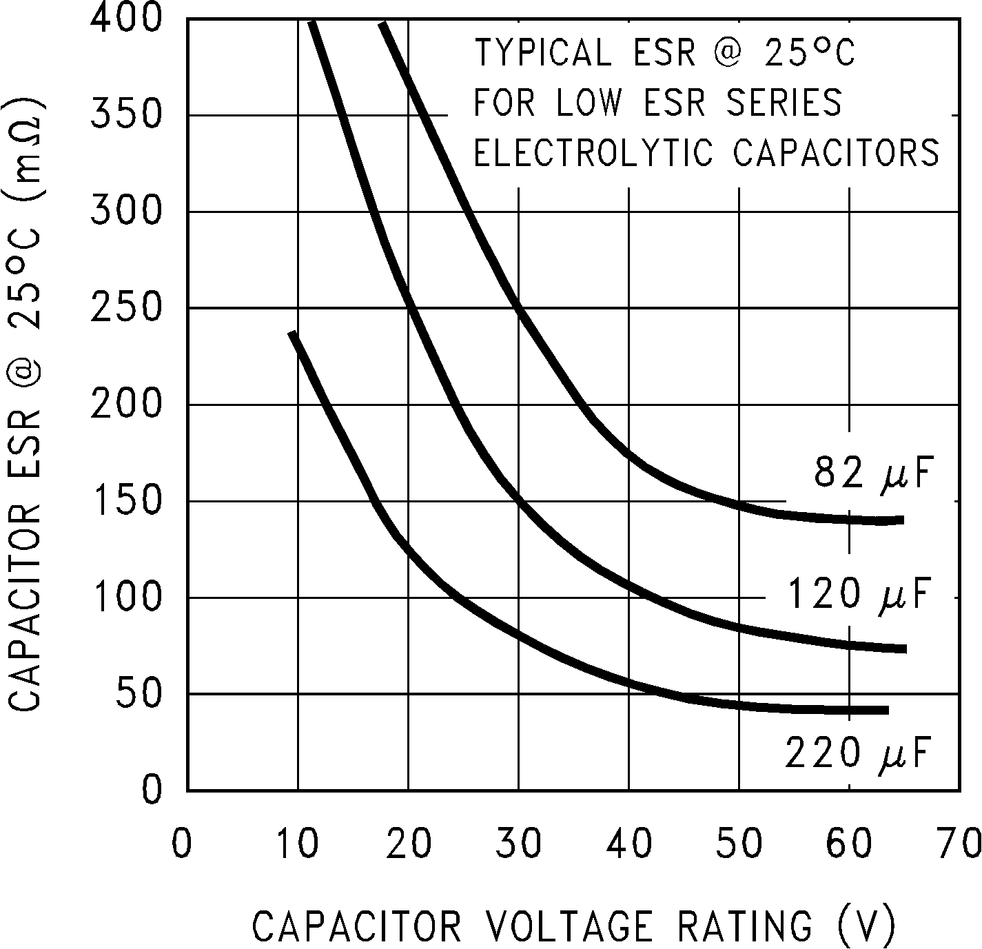
An ESR value of the aluminum electrolytic capacitor is related to the capacitance value and its voltage rating. In most cases, higher voltage electrolytic capacitors have lower ESR values (see Figure 9-2). Often, capacitors with much higher voltage ratings can be required to provide the low ESR values required for low output ripple voltage.
The output capacitor for many different switcher designs often can be satisfied with only three or four different capacitor values and several different voltage ratings. See Table 9-3 and Table 9-4 for typical capacitor values, voltage ratings, and manufacturers capacitor types.
TI does not recommend electrolytic capacitors for temperatures below −25°C. The ESR rises dramatically at cold temperatures and is typically three times as large at −25°C and as much as 10 times as large at −40°C. See Figure 9-3.
Solid tantalum capacitors have a much better ESR specifications for cold temperatures and TI recommends them for temperatures below −25°C.
 Figure 9-2 Capacitor ESR versus Capacitor Voltage Rating (Typical Low-ESR Electrolytic Capacitor)