SNVS523G September 2007 – January 2018 LM3103
PRODUCTION DATA.
- 1 Features
- 2 Applications
- 3 Description
- 4 Revision History
- 5 Pin Configuration and Functions
- 6 Specifications
- 7 Detailed Description
- 8 Applications and Implementation
- 9 Device and Documentation Support
- 10Mechanical, Packaging, and Orderable Information
Package Options
Mechanical Data (Package|Pins)
- PWP|16
Thermal pad, mechanical data (Package|Pins)
- PWP|16
Orderable Information
6.6 Typical Characteristics
All curves are taken at VIN = 18 V with the configuration in the typical application circuit for VOUT = 3.3 V shown in this datasheet. TA = 25°C, unless otherwise specified.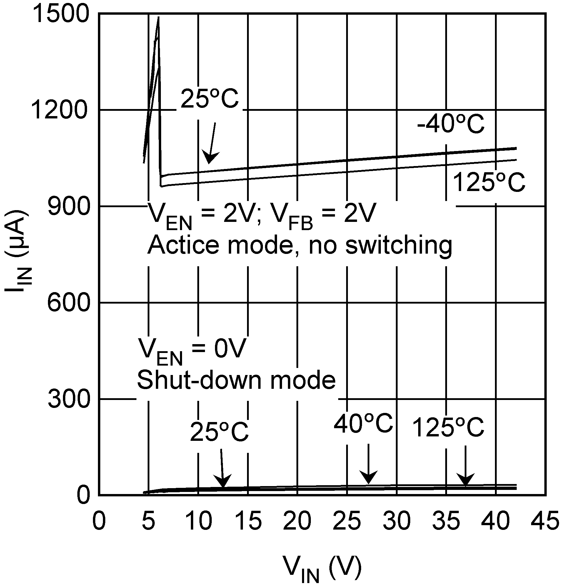 Figure 1. Quiescent Current, IIN vs VIN
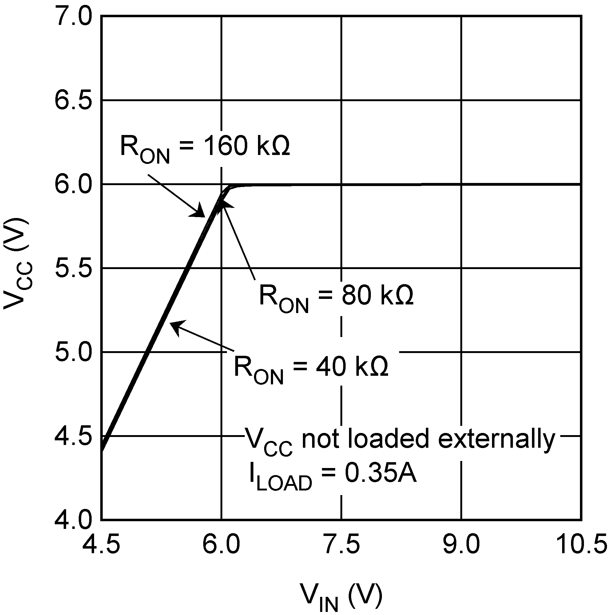 Figure 3. VCC vs VIN
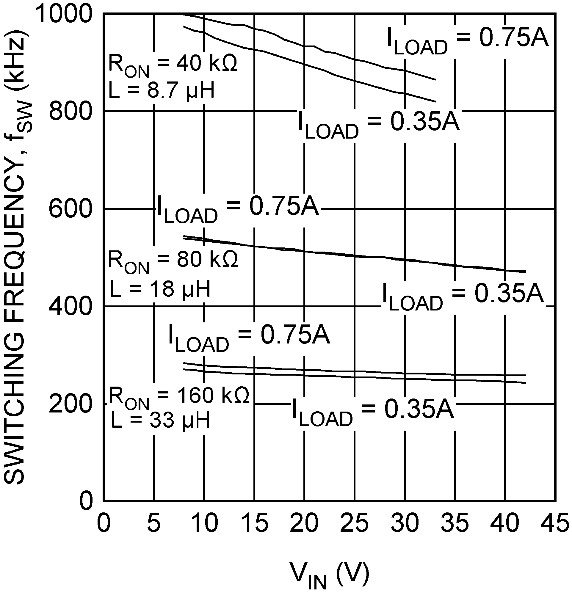 Figure 5. Switching Frequency, fSW vs VIN
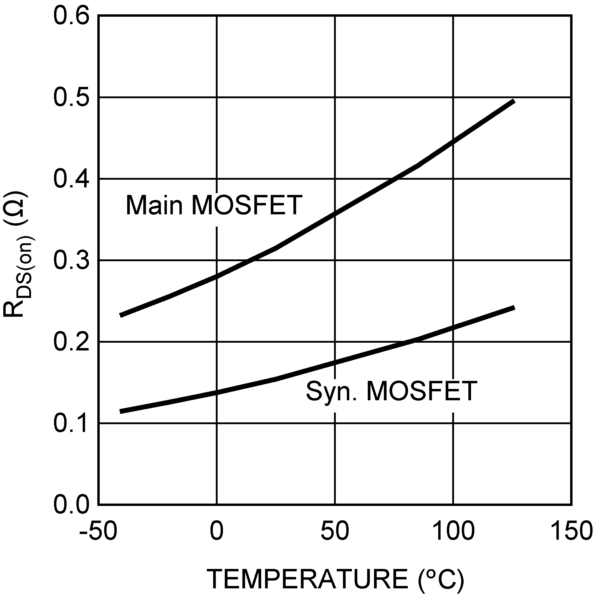 Figure 7. RDS(on) vs Temperature
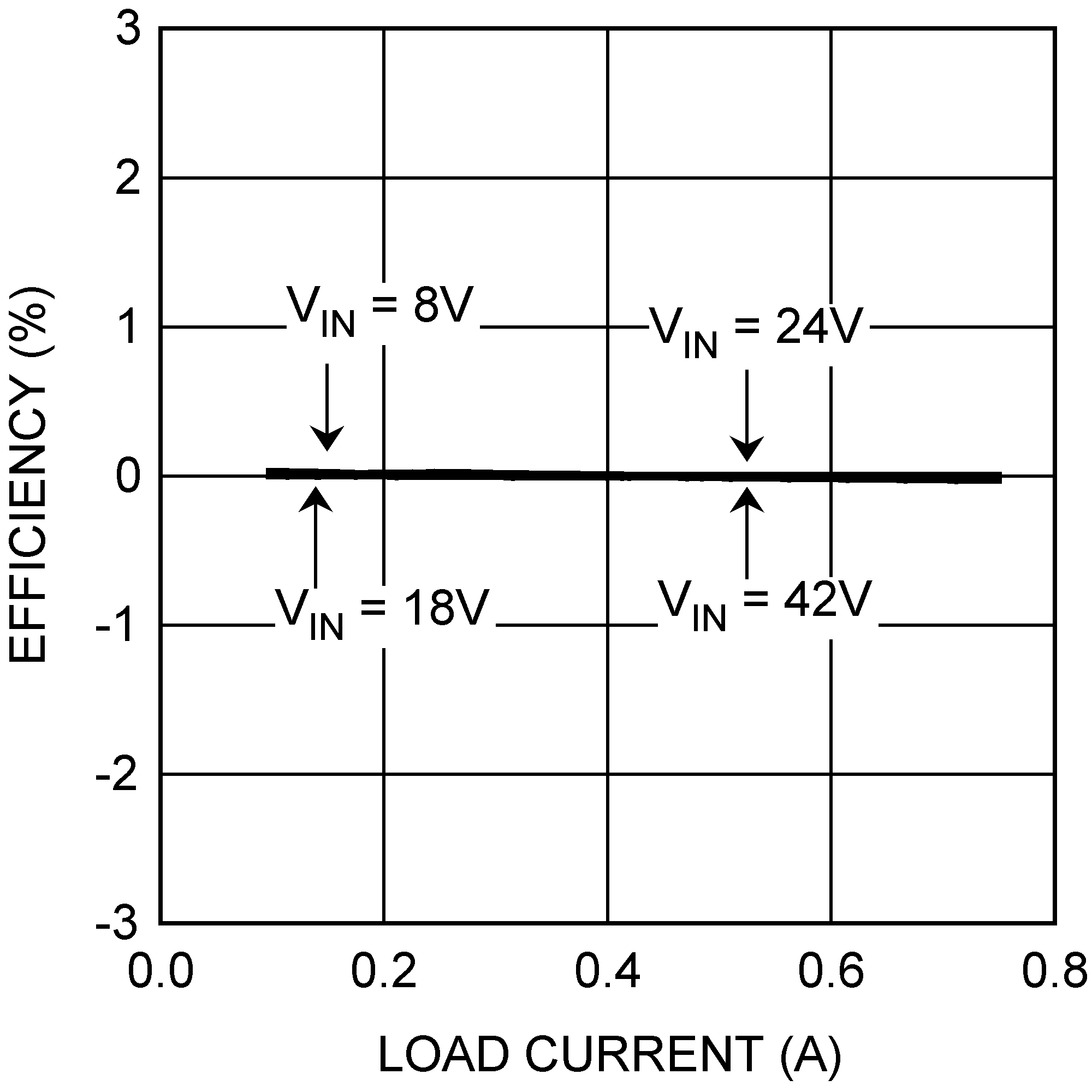 Figure 9. VOUT Regulation vs Load Current (VOUT = 3.3 V)
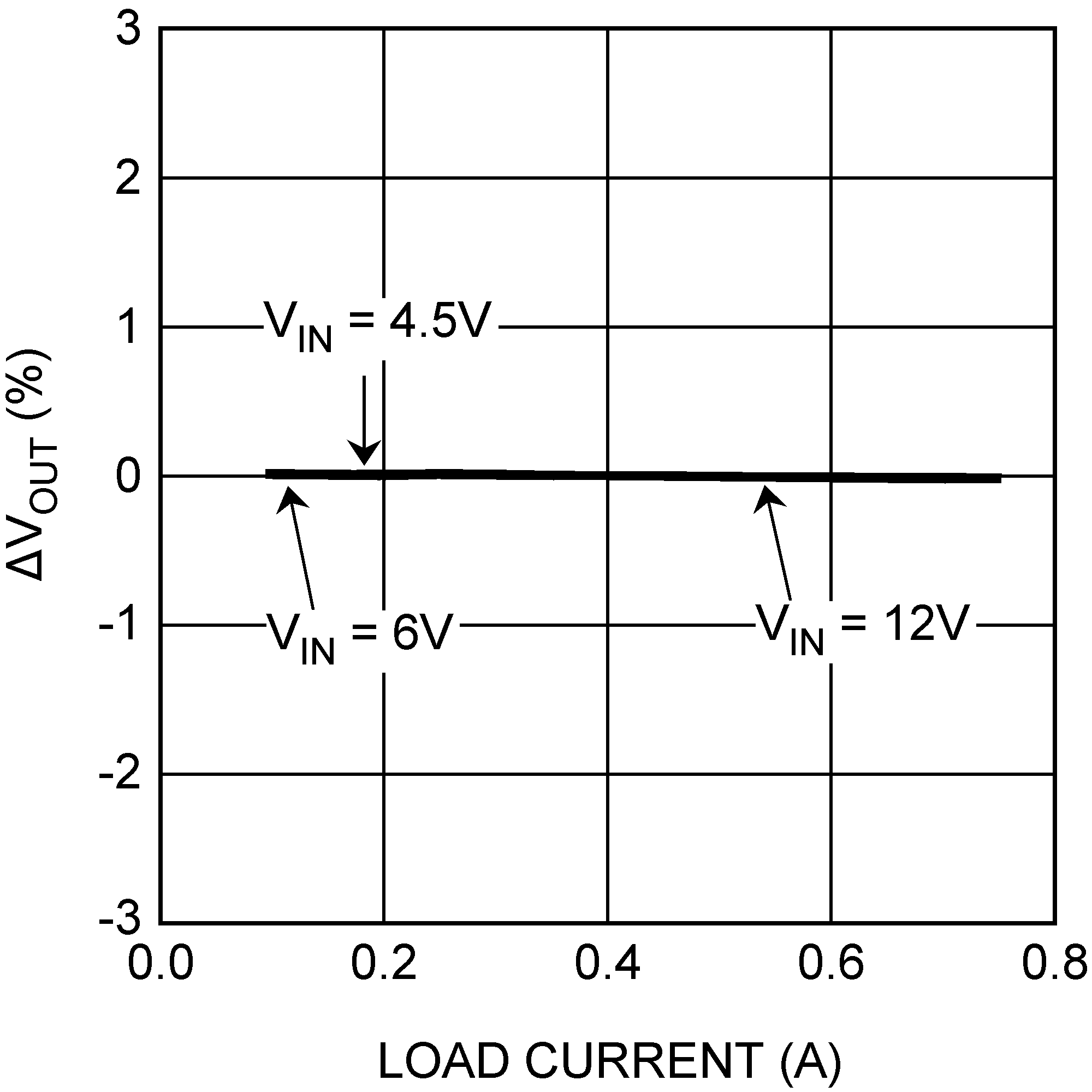
A.
Figure 11. VOUT Regulation vs Load Current (VOUT = 0.6 V)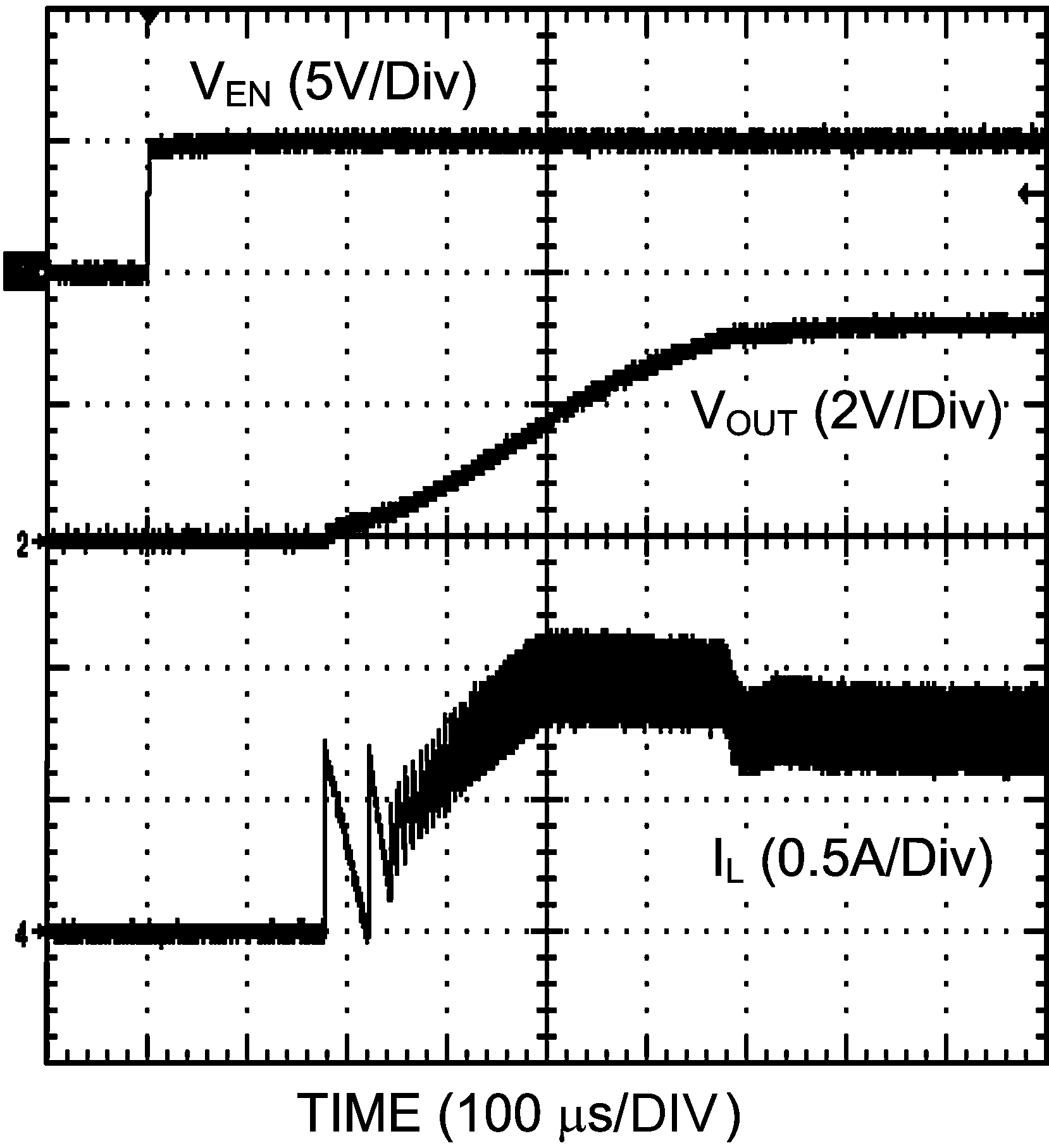 Figure 13. Enable Transient (VOUT = 3.3 V, 0.75 A Loaded)
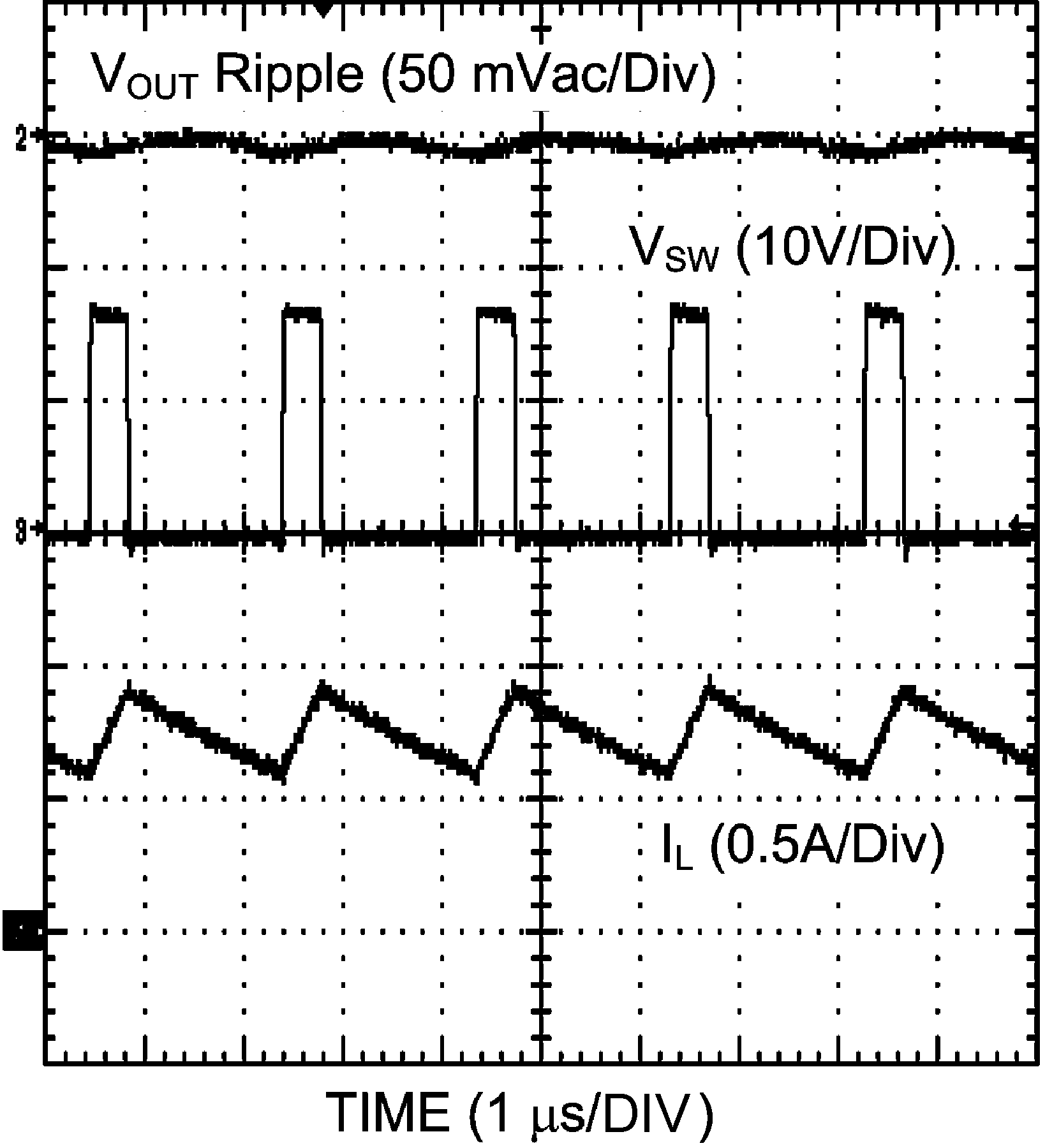 Figure 15. Continuous Mode Operation (VOUT = 3.3 V, 2.5 A Loaded)
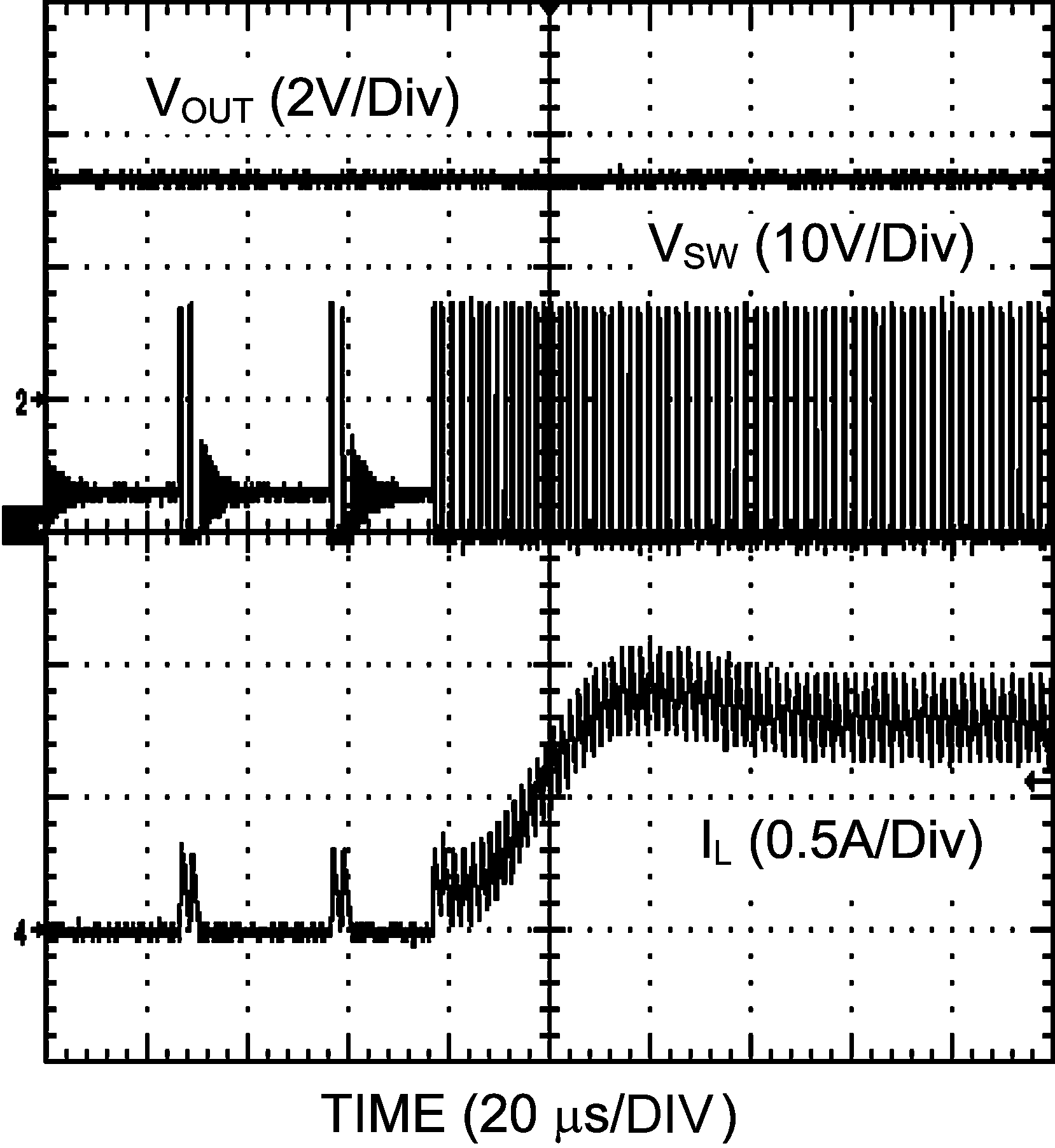 Figure 17. DCM to CCM Transition (VOUT = 3.3 V, 0.01 A - 0.75 A Load)
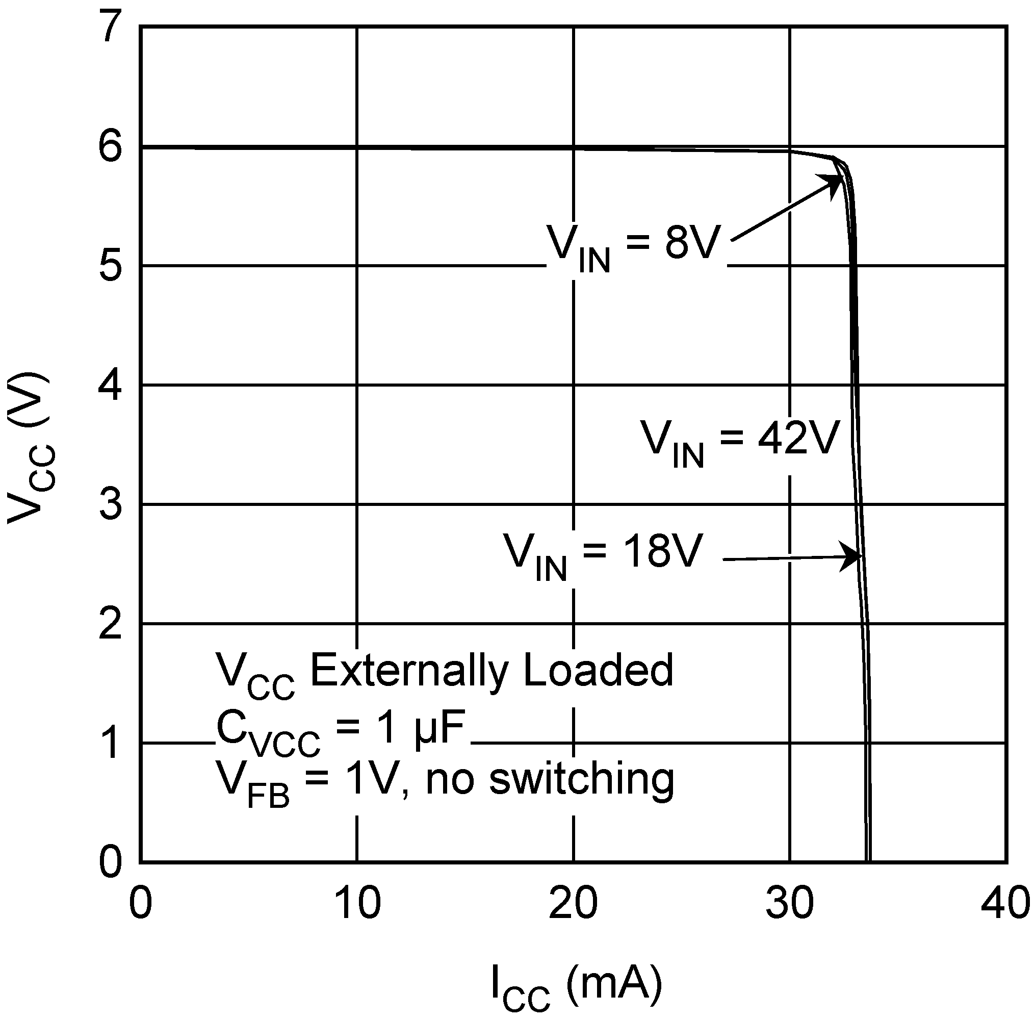 Figure 2. VCC vs ICC
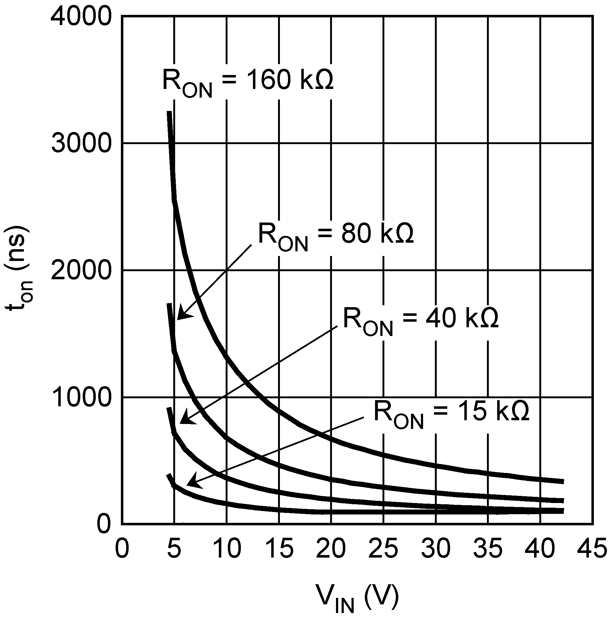 Figure 4. ton vs VIN
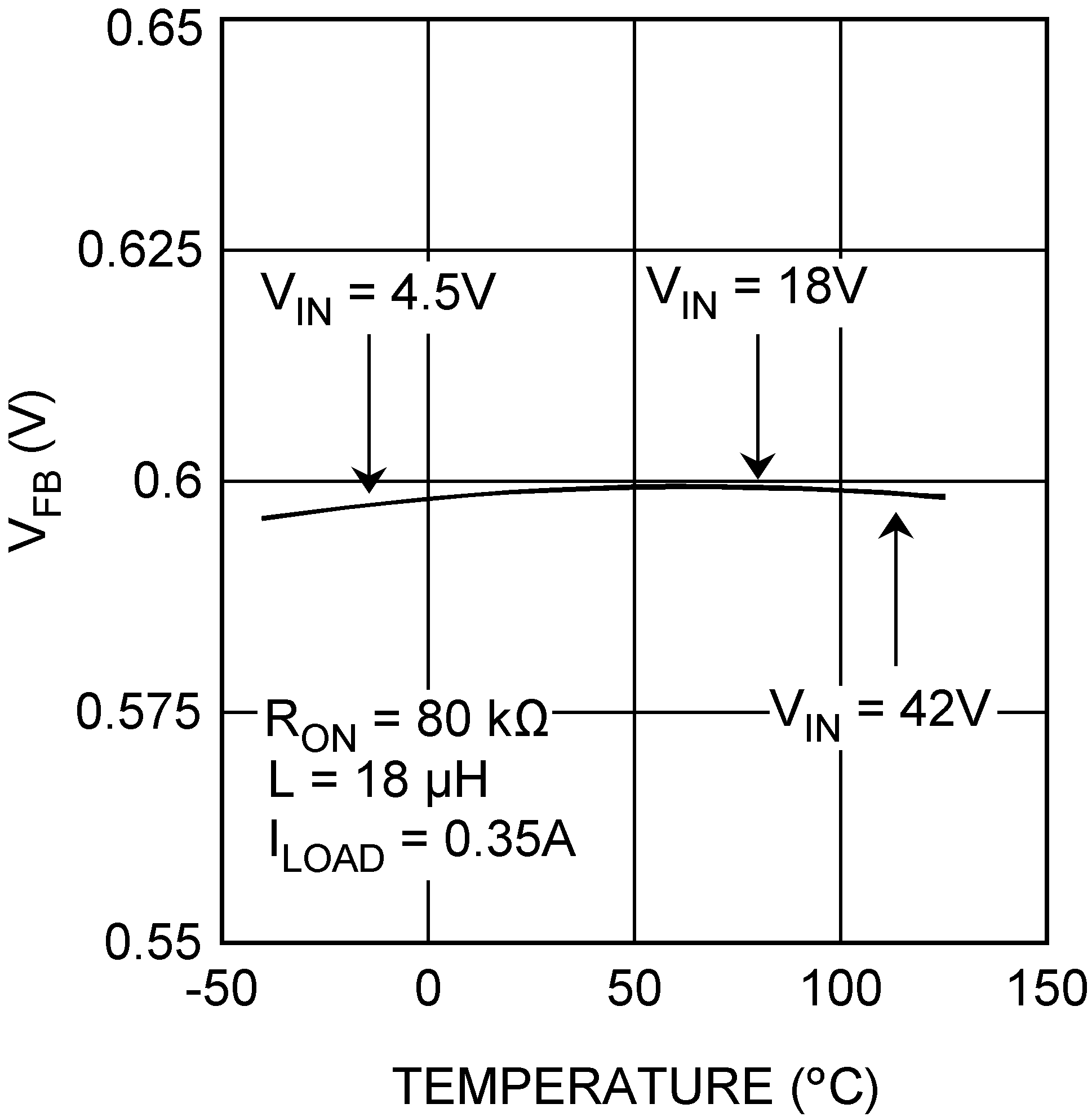 Figure 6. VFB vs Temperature
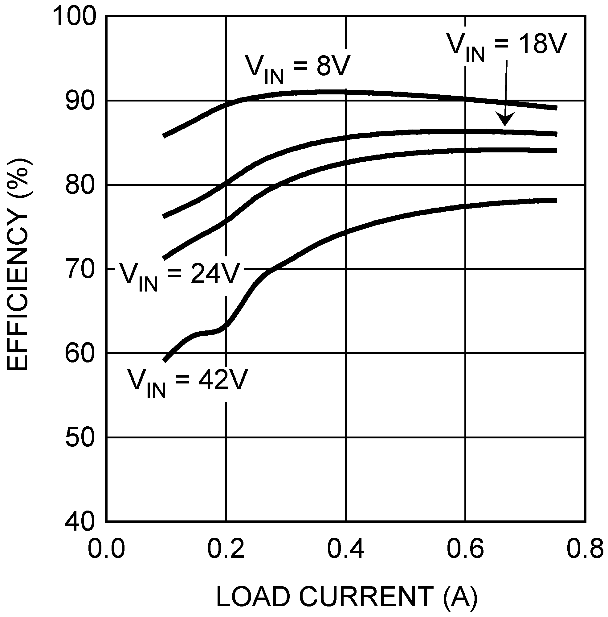 Figure 8. Efficiency vs Load Current (VOUT = 3.3 V)
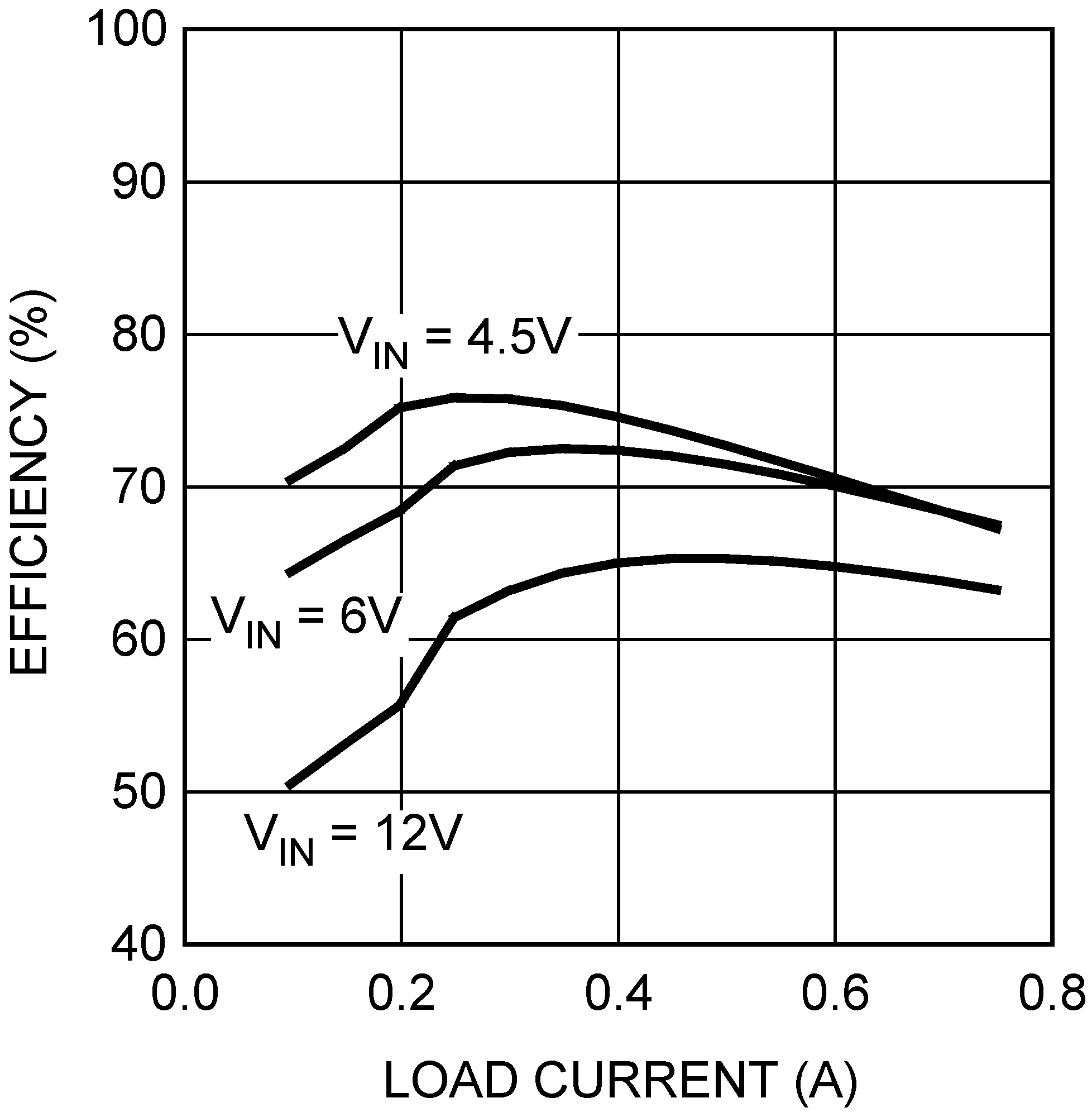 Figure 10. Efficiency vs Load Current (VOUT = 0.6 V)
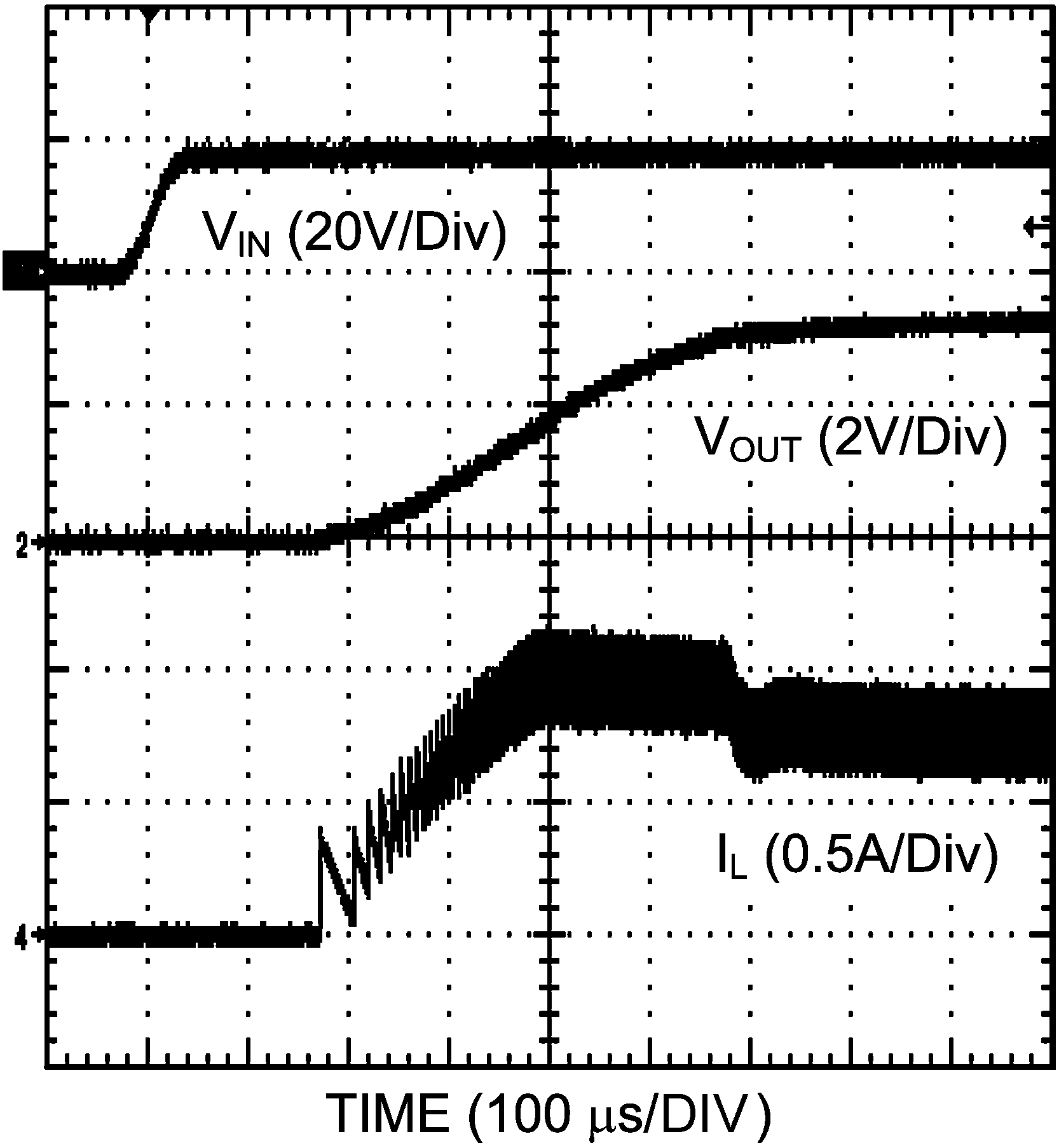
A.
Figure 12. Power Up (VOUT = 3.3 V, 0.75 A Loaded)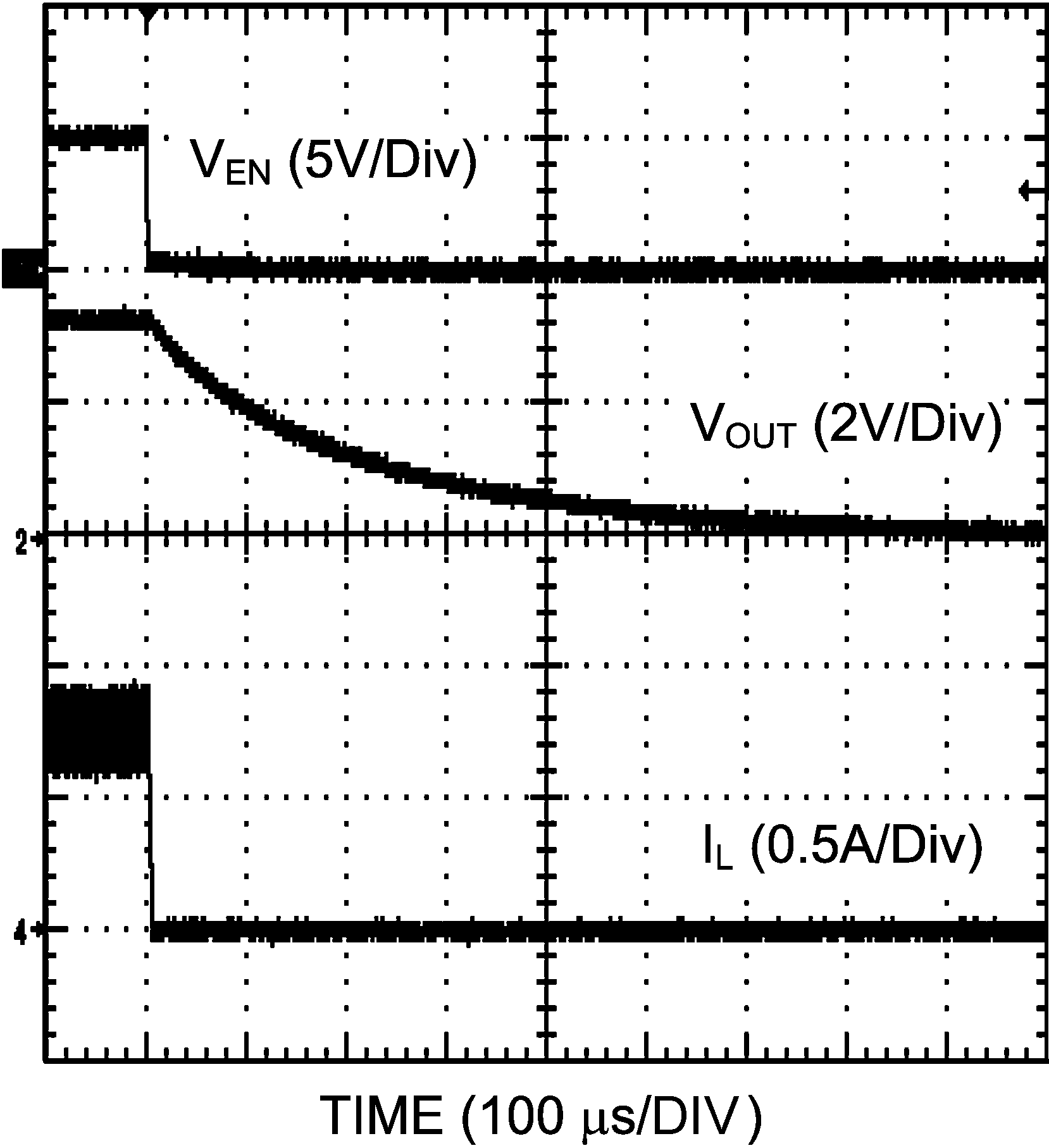 Figure 14. Shutdown Transient (VOUT = 3.3 V, 0.75 A Loaded)
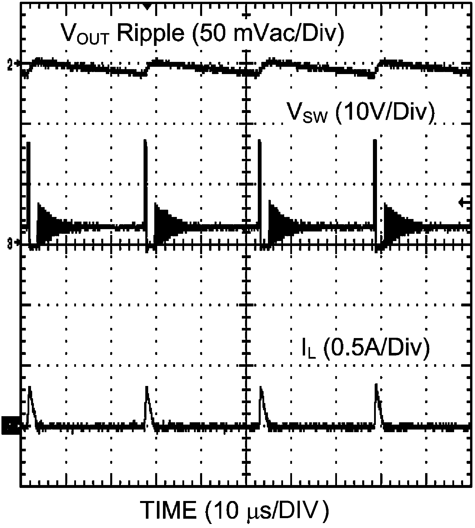 Figure 16. Discontinuous Mode Operation (VOUT = 3.3 V, 0.02 A Loaded)
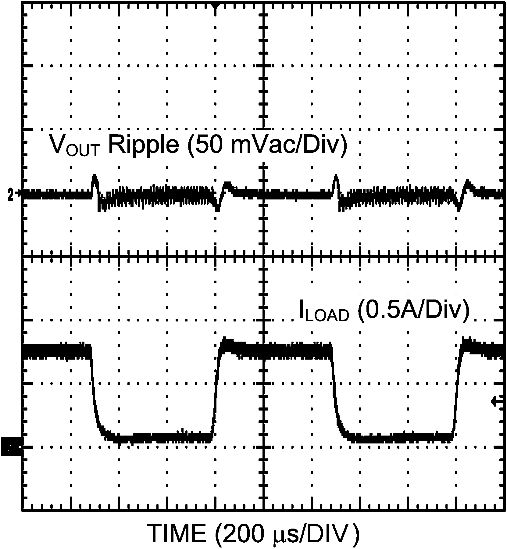 Figure 18. Load Transient (VOUT = 3.3 V, 0.075 A - 0.75 A Load, Current slew-rate: 2.5 A/µs)