SNVS821A January 2014 – March 2014 LM3699
PRODUCTION DATA.
- 1 Features
- 2 Applications
- 3 Description
- 4 Revision History
- 5 Terminal Configuration and Functions
- 6 Specifications
- 7 Detailed Description
- 8 Application and Implementation
- 9 Power Supply Recommendations
- 10Layout
- 11Device and Documentation Support
- 12Mechanical, Packaging, and Orderable Information
Package Options
Mechanical Data (Package|Pins)
- YFQ|12
Thermal pad, mechanical data (Package|Pins)
Orderable Information
8 Application and Implementation
8.1 Application Information
Table 2. Recommended Components
| COMPONENT | MANUFACTURER | VALUE | PART NUMBER | SIZE (mm) | CURRENT/VOLTAGE RATING (RESISTANCE) |
|---|---|---|---|---|---|
| L | TDK | 10 µH | VLF302512MT-100M | 2.5 x 3.0 x 1.2 | 620 mA/0.25 Ω |
| COUT | TDK | 1.0 µF | C2012X5R1E105 | 0805 | 25V |
| CIN | TDK | 2.2 µF | C1005X5R1A225 | 0402 | 10V |
| Diode | On-Semi | Schottky | NSR0240V2T1G | SOD-523 | 40V, 250 mA |
8.2 Typical Application
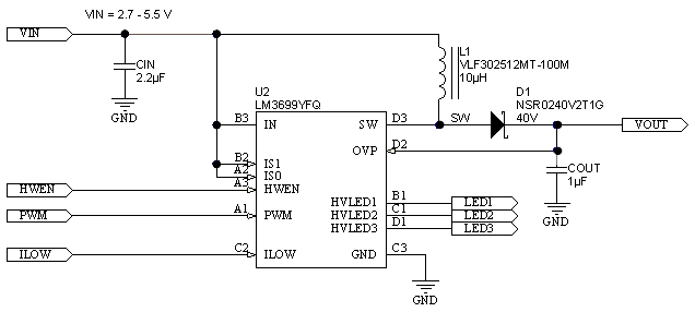 Figure 7. LM3699 Simplified Schematic
8.2.1 Design Requirements
Table 3. Design Parameters
| DESIGN PARAMETER | EXAMPLE VALUE | |||
|---|---|---|---|---|
| Full-scale current setting | 20.2 mA | |||
| Minimum input voltage | 2.7 V | |||
| LED series/parallel configuration | 6s3p | |||
| LED maximum forward voltage (Vf) | 3.5 V | |||
| Efficiency | 75% | |||
8.2.2 Detailed Design Procedure
8.2.2.1 Step-by-Step Design Procedure
The designer needs to know the following:
- Full-scale current setting
- Minimum input voltage
- LED series/parallel configuration
- LED maximum forward voltage (Vf)
- LM3699 efficiency for LED configuration
The full-scale current setting, number of series LEDs, and minimum input voltage are needed in order to calculate the peak input current, maximum output voltage, and maximum required output power. This information guides the designer to determine if the LM3699 can support the required output power and make the appropriate inductor selection for the application.
The LM3699 Boost converter output voltage (VOUT) is calculated as follows: number of series LEDs x Vf + 0.4V
The LM3699 Boost converter output current (IOUT) is calculated as follows: number of parallel LED strings x full-scale current
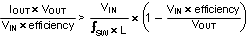
The LM3699 peak input current (IIN_PK) is calculated as follows:
8.2.2.2 Maximum Output Power
The maximum output power of the device is governed by two factors: the peak current limit (ICL = 880 mA min) and the maximum output voltage (VOUT). When the application causes either of these limits to be reached, it is possible that the proper current regulation and matching between LED current strings will not be met.
8.2.2.2.1 Peak Current Limited
In the case of a peak current limited situation, when the peak of the inductor current hits the LM3699 current limit, the NFET switch turns off for the remainder of the switching period. If this happens each switching cycle the LM3699 regulates the peak of the inductor current instead of the headroom across the current sinks. This can result in the dropout of the current sinks, and the LED current dropping below its programmed level.
The peak current (IPEAK) in a boost converter is dependent on the value of the inductor, total LED current in the boost (IOUT), the boost output voltage (VOUT) (which is the highest voltage LED string + VHR ), the input voltage (VIN), the switching frequency (ƒSW), and the efficiency (Output Power/Input Power). Additionally, the peak current is different depending on whether the inductor current is continuous during the entire switching period (CCM), or discontinuous (DCM) where it goes to 0 before the switching period ends. For CCM, the peak inductor current is given by:
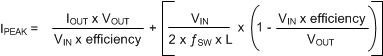
For DCM the peak inductor current is given by:
To determine which mode the circuit is operating in (CCM or DCM) a calculation must be done to test whether the inductor current ripple is less than the anticipated input current (IIN). If ΔIL is less than IIN, then the device is operating in CCM. If ΔIL is greater than IIN then the device is operating in DCM.
Typically at currents high enough to reach the LM3699 peak current limit, the device operates in CCM.
Figure 8 shows the output current derating for a 10-µH and a 22-µH inductor using 75% and 80% efficiency estimates. These plots take equations (2) and (3) from above and plot IOUT with varying VIN using a constant peak current of 880 mA (ICL_MIN) and 1-MHz switching frequency. Using these curves can help the user understand the impact of VIN, inductance, and efficiency on the maximum output current. A 10-µH inductor can typically be a smaller device with lower on resistance, but the peak currents will be higher. A 22-µH inductor provides for lower peak currents, but to match the DC resistance of a 10-µH inductor requires a larger sized device.
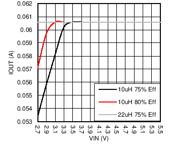 Figure 8. Maximum Output Power Vs Inductance And Efficiency
8.2.2.2.2 Output Voltage Limited
If a output voltage limited situation occurs, when the boost output voltage hits the LM3699 OVP threshold, the NFET turns off and stays off until the output voltage falls below the hysteresis level (typically 1 V below the OVP threshold). This results in the boost converter regulating the output voltage to the OVP threshold, causing the current sinks to go into dropout. The LM3699 OVP setting supports LED strings up to 6 series LEDs (Vƒmax = 3.5 V).
8.2.2.3 Boost Inductor Selection
The boost converter operates using either a 10-µH or 22-µH inductor. The inductor selected must have a saturation current greater than the peak operating current.
8.2.2.4 Output Capacitor Selection
The LM3699 inductive boost converter requires a 1.0-µF X5R or X7R 50V (0805 size) ceramic capacitor to filter the output voltage. Pay careful attention to the capacitor tolerance and DC bias response. Smaller body-size 1.0-µF ceramic capacitors or 25-V, 1.0-µF ceramic capacitors can be used, but for proper operation the degradation in capacitance due to tolerance, DC bias, and temperature should stay above 0.4 µF. This might require placing two devices in parallel in order to maintain the required output capacitance over the device operating range and series LED configuration.
8.2.2.5 Schottky Diode Selection
The Schottky diode must have a reverse breakdown voltage greater than the LM3699’s maximum output voltage. Additionally, the diode must have an average current rating high enough to handle the LM3699’s maximum output current, and at the same time the diode peak current rating must be high enough to handle the peak inductor current. Schottky diodes are required due to their lower forward voltage drop (0.3 V to 0.5 V) and their fast recovery time.
8.2.2.6 Input Capacitor Selection
The LM3699 inductive boost converter requires a 2.2-µF X5R or X7R ceramic capacitor to filter the input voltage. The input capacitor filters the inductor current ripple and the internal MOSFET driver currents during turnon of the internal power switch.
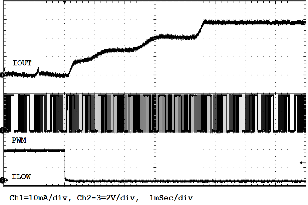
8.2.3 Application Performance Plots
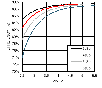
VIN = 3.6 V, LEDs are WLEDs part # SML-312WBCW(A), Typical Application Circuit with L = TDK (VLF302512, 10 µH, 22 µH where specified), Schottky = On-Semi (NSR0240V2T1G), TA = 25°C unless otherwise specified. Efficiency is given as (VOUT × (IHVLED1 + IHVLED2+ IHVLED3))/(VIN × IIN), matching curves are given as (ΔILED_MAX/ILED_AVE).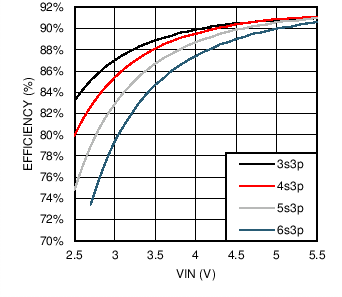
| L = 22 µH | 20 mA/String |
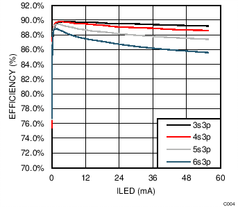 Figure 11. LED Efficiency vs ILED
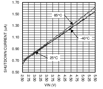 Figure 13. Shutdown Current vs VIN
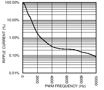
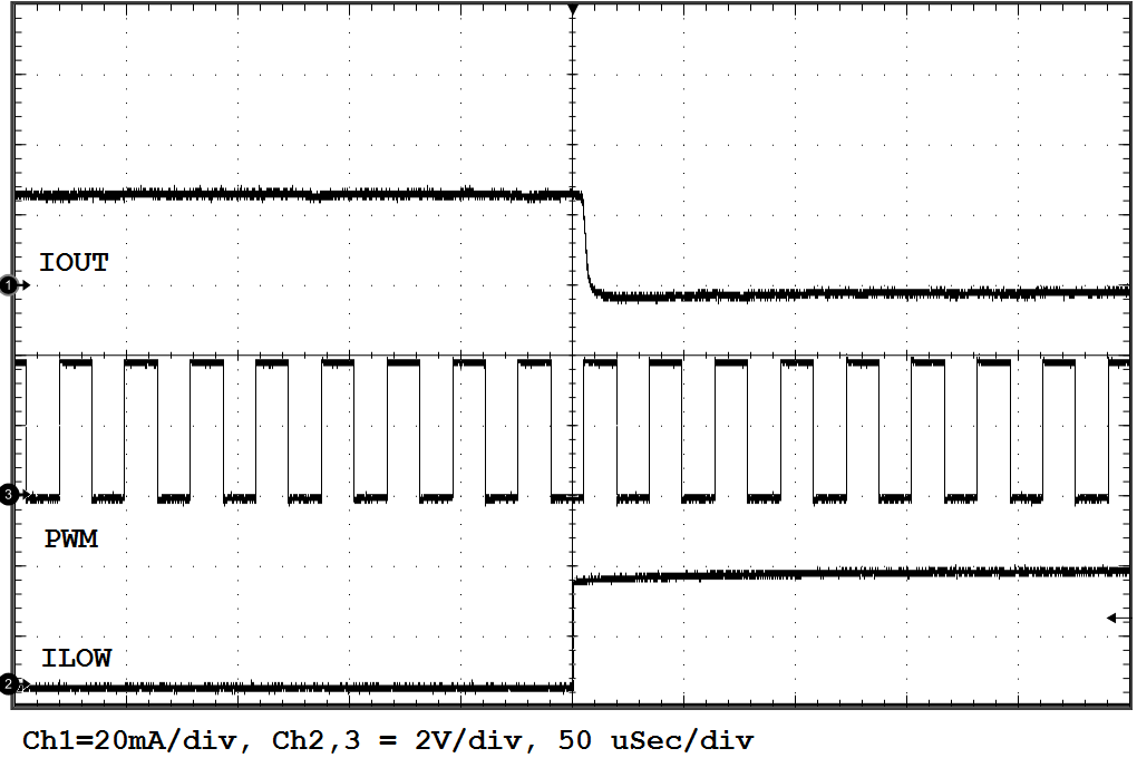
| DPWM = 50% | 3 x 6 LEDs | 20 mA/String |
| DPWM = 0% | 3 x 6 LEDs | 20 mA/String |
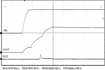
| 3p6s | 20.2 mA/String | DPWM = 100% |
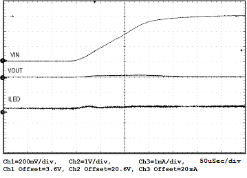
| 3.6 V to 4.2 V |
| 3p6s | 20.2 mA/String | DPWM = 50% |
| L = 10 µH | 20 mA/String |
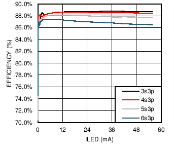 Figure 12. LED Efficiency vs ILED
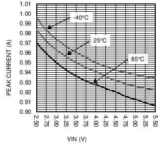 Figure 14. Open Loop Current Limit vs VIN
| DPWM = 100% | 3 x 6 LEDs | 20 mA/String |
| 3p6s | DPWM = 30% to 90% | ƒ = 10 kHz |
| 20.2 mA/String |
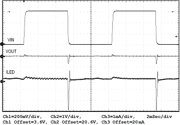
| 3p6s | 20.2 mA/String | DPWM = 100% |
| 4.2 V to 3.6 V |
| 3p6s | 20.2 mA/String | DPWM = 50% |