SNVS821A January 2014 – March 2014 LM3699
PRODUCTION DATA.
- 1 Features
- 2 Applications
- 3 Description
- 4 Revision History
- 5 Terminal Configuration and Functions
- 6 Specifications
- 7 Detailed Description
- 8 Application and Implementation
- 9 Power Supply Recommendations
- 10Layout
- 11Device and Documentation Support
- 12Mechanical, Packaging, and Orderable Information
Package Options
Mechanical Data (Package|Pins)
- YFQ|12
Thermal pad, mechanical data (Package|Pins)
Orderable Information
7 Detailed Description
7.1 Overview
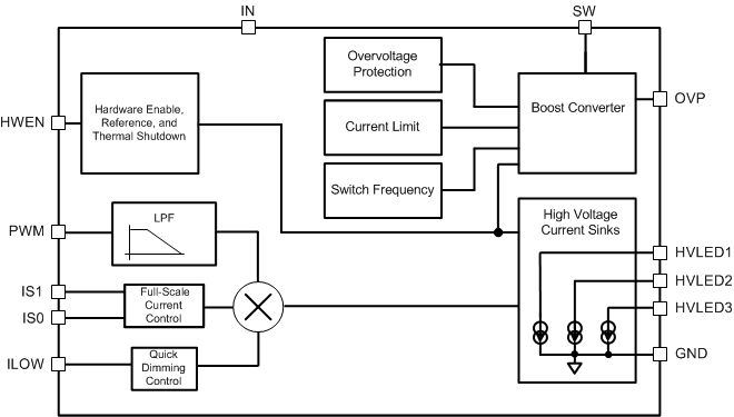
The LM3699 provides power for three high-voltage LED strings. The high-voltage LED strings are powered from an integrated boost converter. The LED current is directly controlled by a Pulse Width Modulation (PWM) input.
7.2 Functional Block Diagram
7.3 Feature Description
7.3.1 PWM Input
The active high PWM input is filtered by an internal low-pass filter, then converted to an analog control voltage to set the current level on the current sink outputs. The PWM input is high-impedance and cannot be left floating.
7.3.1.1 PWM Input Frequency Range
The usable input frequency range for the PWM input is governed on the low end by the cutoff frequency of the internal low-pass filter (540 Hz, Q = 0.33) and on the high end by the propagation delays through the internal logic. For frequencies below 2 kHz the current ripple begins to become a larger portion of the DC LED current. Additionally, at lower PWM frequencies the boost output voltage ripple increases, causing a non-linear response from the PWM duty cycle to the average LED current due to the response time of the boost. For the best response of current vs. duty cycle, the PWM input frequency should be kept between 2 kHz and 100 kHz.
7.3.1.2 PWM Low Detect
The LM3699 incorporates a feature to detect when the PWM input duty cycle is near zero. This feature requires that the minimum PWM input pulse width be greater than tPWM (see Electrical Characteristics). A PWM input pulse width less than tPWM can result in the current sink outputs turning on and off resulting in flicker on the LEDs.
7.3.2 HWEN Input
HWEN is the global hardware enable to the LM3699 and must be driven high to enable the device. HWEN is a high-impedance input, so it cannot be left floating. When HWEN is driven low the LM3699 is placed in shutdown, and the boost converter and all the HVLED current sinks are turned off.
7.3.3 Current Select Inputs (IS1 And IS0)
The current select inputs IS1 and IS0 select the maximum full-scale current (ifs). These digital inputs are static and must not change state when HWEN > VIL. IS1 and IS0 are high-impedance inputs so they cannot be left floating. The terminals IS1 and IS0 can be connected directly to IN or GND and do not require an external pullup/pulldown resistor. The full-scale current is set according to Table 1:
Table 1. Full-Scale Current vs Current Select Inputs IS1 and IS0
| IS1 | IS0 | FULL-SCALE CURRENT (ifs) (mA) |
|---|---|---|
| 0 | 0 | 15.4 |
| 0 | 1 | 17.0 |
| 1 | 0 | 18.6 |
| 1 | 1 | 20.2 |
7.3.4 ILOW Input
The ILOW feature provides a way to quickly reduce the LED current. This feature can be used to dim the LCD backlight during camera flash operation without changing the PWM duty cycle. ILOW is a high-impedance input so it cannot be left floating. When ILOW is driven high, the high-voltage current sink outputs are approximately equal to (ifs x DPWM x 5%). When ILOW is driven low, the high-voltage current sinks are a function of the full-scale current setting and the PWM input duty cycle. If ILOW is not required the input should be connected to GND.
7.3.5 Thermal Shutdown
The LM3699 contains a thermal shutdown protection. In the event the die temperature reaches 140°C (typ), the boost converter and current sink outputs shut down until the die temperature drops to typically 125°C.
7.4 Device Functional Modes
7.4.1 Operation with an Unused Current Sink
If one of the current sink outputs is not connected to a LED string the terminal must be connected to VIN. This ensures that the boost converter regulates the headroom voltage on the highest voltage LED string.