SNVS821A January 2014 – March 2014 LM3699
PRODUCTION DATA.
- 1 Features
- 2 Applications
- 3 Description
- 4 Revision History
- 5 Terminal Configuration and Functions
- 6 Specifications
- 7 Detailed Description
- 8 Application and Implementation
- 9 Power Supply Recommendations
- 10Layout
- 11Device and Documentation Support
- 12Mechanical, Packaging, and Orderable Information
Package Options
Mechanical Data (Package|Pins)
- YFQ|12
Thermal pad, mechanical data (Package|Pins)
Orderable Information
10 Layout
10.1 Layout Guidelines
The LM3699 inductive boost converter sees a high switched voltage (up to 24 V) at the SW terminal, as well as a step current (up to 1 A) through the Schottky diode and output capacitor each switching cycle. The high switching voltage can create interference into nearby nodes due to electric field coupling (I = CdV/dt). The large step current through the diode and the output capacitor can cause a large voltage spike at the SW and OVP terminals due to parasitic inductance in the step current conducting path (V = Ldi/dt). Board layout guidelines are geared towards minimizing this electric field coupling and conducted noise. Figure 24 highlights these two noise-generating components.
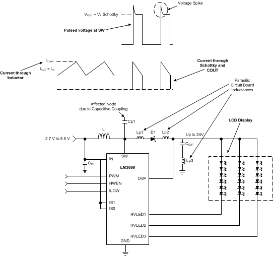 Figure 24. LM3699 Inductive Boost Converter Showing Pulsed Voltage At SW (High dv/dt) And Current Through Schottky And COUT (High di/dt)
The following list details the main (layout sensitive) areas of the LM3699 inductive boost converter in order of decreasing importance:
- Output Capacitor
- Schottky Cathode to COUT+
- COUT− to GND
- Schottky Diode
- SW Terminal to Schottky Anode
- Schottky Cathode to COUT+
- Inductor
- SW Node PCB capacitance to other traces
- Input Capacitor
- CIN+ to IN terminal
10.1.1 Boost Output Capacitor Placement
Because the output capacitor is in the path of the inductor current discharge path, a high-current step from 0 to IPEAK occurs each time the switch turns off and the Schottky diode turns on. Any inductance along this series path from the cathode of the diode through COUT and back into the LM3699 GND terminal contributes to voltage spikes (VSPIKE = LP_ × di/dt) at SW and OUT. These spikes can potentially over-voltage the SW terminal, or feed through to GND. To avoid this, COUT+ must be connected as close as possible to the Cathode of the Schottky diode, and COUT− must be connected as close as possible to the LM3699 GND terminal. The best placement for COUT is on the same layer as the LM3699 so as to avoid any vias that can add excessive series inductance.
10.1.2 Schottky Diode Placement
In the boost circuit of the device the Schottky diode is in the path of the inductor current discharge. As a result the Schottky diode sees a high-current step from 0 to IPEAK each time the switch turns off and the diode turns on. Any inductance in series with the diode may cause a voltage spike (VSPIKE = LP_ × di/dt) at SW and OUT. This can potentially over-voltage the SW terminal, or feed through to VOUT and through the output capacitor and into GND. Connecting the anode of the diode as close as possible to the SW terminal and the cathode of the diode as close as possible to COUT+ reduces the inductance (LP_) and minimize these voltage spikes.
10.1.3 Inductor Placement
The node where the inductor connects to the LM3699 SW terminal has 2 issues. First, a large switched voltage (0 to VOUT + VF_SCHOTTKY) appears on this node every switching cycle. This switched voltage can be capacitively coupled into nearby nodes. Second, there is a relatively large current (input current) on the traces connecting the input supply to the inductor and connecting the inductor to the SW terminal. Any resistance in this path can cause voltage drops that can negatively affect efficiency and reduce the input operating voltage range.
To reduce the capacitive coupling of the signal on SW into nearby traces, the SW terminal-to-inductor connection must be minimized in area. This limits the PCB capacitance from SW to other traces. Additionally, high-impedance nodes that are more susceptible to electric field coupling need to be routed away from SW and not directly adjacent or beneath. This is especially true for traces such as IS1, IS0, ILOW, HWEN, and PWM. A GND plane placed directly below SW greatly reduce the capacitance from SW into nearby traces.
Lastly, limit the trace resistance of the VBATT-to-inductor connection and from the inductor-to-SW connection, by use of short, wide traces.
10.1.4 Boost Input Capacitor Placement
For the LM3699 boost converter, the input capacitor filters the inductor current ripple and the internal MOSFET driver currents during turnon of the internal power switch. The driver current requirement can range from 50 mA at 2.7 V to over 200 mA at 5.5 V with fast durations of approximately 10 ns to 20 ns. This appears as high di/dt current pulses coming from the input capacitor each time the switch turns on. Close placement of the input capacitor to the IN terminal and to the GND terminal is critical since any series inductance between IN and CIN+ or CIN− and GND can create voltage spikes that could appear on the VIN supply line and in the GND plane.
10.2 Layout Example
Figure 25 requires two PCB layers and is optimized for the GND connection.
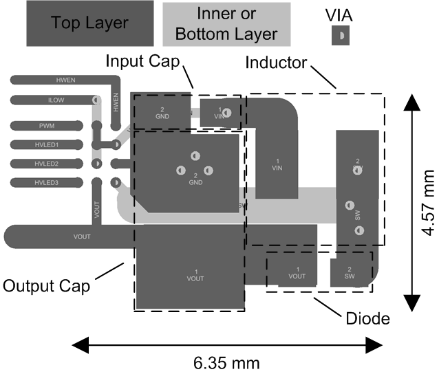 Figure 25. LM3699 GND Optimized Layout Example