SNVS821A January 2014 – March 2014 LM3699
PRODUCTION DATA.
- 1 Features
- 2 Applications
- 3 Description
- 4 Revision History
- 5 Terminal Configuration and Functions
- 6 Specifications
- 7 Detailed Description
- 8 Application and Implementation
- 9 Power Supply Recommendations
- 10Layout
- 11Device and Documentation Support
- 12Mechanical, Packaging, and Orderable Information
Package Options
Mechanical Data (Package|Pins)
- YFQ|12
Thermal pad, mechanical data (Package|Pins)
Orderable Information
6 Specifications
6.1 Absolute Maximum Ratings
over operating free-air temperature range (unless otherwise noted) (1)(2)| MIN | MAX | UNIT | ||
|---|---|---|---|---|
| VIN to GND | −0.3V | 6 | V | |
| VSW, VOVP, VHVLED1, VHVLED2, VHVLED3 to GND | −0.3V | 45 | ||
| VIS1, VIS0, VILOW, VPWM to GND | −0.3V | 6 | ||
| VHWEN to GND | −0.3V | 6 | ||
| Continuous power dissipation | Internally Limited | |||
| Maximum lead temperature (soldering) | 260 (peak) | °C | ||
| Junction temperature (TJ-MAX) | 150 | |||
(1) Stresses beyond those listed under Absolute Maximum Ratings may cause permanent damage to the device. These are stress ratings only, which do not imply functional operation of the device at these or any other conditions beyond those indicated under Recommended Operating Conditions. Exposure to absolute-maximum-rated conditions for extended periods may affect device reliability.
(2) All voltages are with respect to the potential at the GND terminal.
6.2 Handling Ratings
| MIN | MAX | UNIT | ||
|---|---|---|---|---|
| Storage temperature range | −65 | 150 | °C | |
| ESD Ratings(1) | Human body model (HBM)(2) | 2.0 | kV | |
| Charged device model (CDM)(3) | 1500 | V | ||
(1) Electrostatic discharge (ESD) to measure device sensitivity and immunity to damage caused by assembly line electrostatic discharges in to the device.
(2) Level listed above is the passing level per ANSI, ESDA, and JEDEC JS-001. JEDEC document JEP155 states that 500-V HBM allows safe manufacturing with a standard ESD control process.
(3) Level listed above is the passing level per EIA-JEDEC JESD22-C101. JEDEC document JEP157 states that 250-V CDM allows safe manufacturing with a standard ESD control process.
6.3 Recommended Operating Conditions
over operating free-air temperature range (unless otherwise noted)| MIN | MAX | UNIT | ||
|---|---|---|---|---|
| VIN to GND | 2.7 | 5.5 | V | |
| VSW, VOVP, VHVLED1, VVHLED2, VVHLED3 to GND | 0 | 24 | ||
| Junction temperature (TJ) (1)(2) | −40 | 125 | °C | |
(1) Internal thermal shutdown circuitry protects the device from permanent damage. Thermal shutdown engages at TJ= 140°C (typ) and disengages at TJ = 125°C (typ).
(2) In applications where high power dissipation and/or poor package thermal resistance is present, the maximum ambient temperature may have to be derated. Maximum ambient temperature (TA-MAX) is dependent on the maximum operating junction temperature (TJ-MAX-OP = 125°C), the maximum power dissipation of the device in the application (PD-MAX), and the junction-to ambient thermal resistance of the part/package in the application (θJA), as given by the following equation: TA-MAX = TJ-MAX-OP – (θJA × PD-MAX).
6.4 Thermal Information
| THERMAL METRIC(1) | DSBGA | UNIT | |
|---|---|---|---|
| (12 TERMINALS) | |||
| RθJA | Junction-to-ambient thermal resistance | 55 | °C/W |
(1) For more information about traditional and new thermal metrics, see the IC Package Thermal Metrics application report, SPRA953.
6.5 Electrical Characteristics
Limits apply over the full operating ambient temperature range (−40°C ≤ TA ≤ 85°C) and VIN = 3.6V, unless otherwise specified.(1)(2)| SYMBOL | PARAMETER | TEST CONDITIONS | MIN | TYP | MAX | UNIT |
|---|---|---|---|---|---|---|
| General | ||||||
| ISHDN | Shutdown current | 2.7 V ≤ VIN ≤ 5.5 V, HWEN = GND | 3.0 | µA | ||
| 2.7 V ≤ VIN ≤ 5.5 V, HWEN = GND, TA = 25°C |
1 | |||||
| TSD | Thermal shutdown | 140 | °C | |||
| Hysteresis | 15 | |||||
| Boost Converter | ||||||
| IHVLED(1/2/3) | Output current regulation (HVLED1, HVLED2, HVLED3) | 2.7 V ≤ VIN ≤ 5.5 V, ILOW = GND, IS0 = IS1 = VIN, PWM Duty Cycle = 100% |
18.38 | 22.02 | mA | |
| 2.7 V ≤ VIN ≤ 5.5 V, ILOW = GND, IS0 = IS1 = VIN, PWM Duty Cycle = 100% TA = 25°C |
20.2 | |||||
| ILOW = GND, IS0 = IS1 = VIN, PWM Duty Cycle = 100% TA = 25°C |
18.7 | 21.58 | ||||
| ILOW = GND, IS0 = IS1 = VIN, PWM Duty Cycle = 100%, TA = 25°C |
20.2 | |||||
| 3.0 V ≤ VIN ≤ 4.5 V, ILOW = GND, IS0 = IS1 = VIN, PWM Duty Cycle = 100% TA = 25°C |
18.63 | 21.58 | ||||
| 3.0 V ≤ VIN ≤ 4.5 V, ILOW = GND, IS0 = IS1 = VIN, PWM Duty Cycle = 100% TA = 25°C |
20.2 | |||||
| IMATCH_HV | HVLED matching (HVLED1 to HVLED2 or HVLED2 to HVLED3 or HVLED1 to HVLED3) (3) |
2.7 V ≤ VIN ≤ 5.5 V, ILOW = GND, IS0 = IS1 = VIN, PWM Duty Cycle = 100% |
–2.5% | 2.5% | ||
| ILOW = GND, IS0 = IS1 = VIN, PWM Duty Cycle = 100%, TA = 25°C |
–2% | 1.7% | ||||
| 3.0 V ≤ VIN ≤ 4.5 V, ILOW = GND, IS0 = IS1 = VIN, PWM Duty Cycle = 100% |
–2.5% | 2.5% | ||||
| VREG_CS | Regulated current sink headroom voltage | ILOW = GND, IS0 = IS1 = VIN, PWM Duty Cycle = 100%, TA = 25°C |
400 | mV | ||
| VHR_MIN | Minimum current sink headroom voltage for HVLED current sinks | ILED = 95% of nominal, ILOW = GND, IS0 = IS1 = VIN, PWM Duty Cycle = 100% | 275 | |||
| ILED = 95% of nominal, ILOW = GND, IS0 = IS1 = VIN, PWM Duty Cycle = 100% TA = 25°C |
190 | |||||
| RDSON | NMOS switch on resistance | ISW = 500 mA, TA = 25°C | 0.3 | Ω | ||
| ICL_BOOST | NMOS Switch Current Limit | 880 | 1120 | mA | ||
| TA = 25°C | 1000 | |||||
| VOVP | Output overvoltage protection | ON threshold, 2.7 V ≤ VIN ≤ 5.5 V | 23 | 25 | V | |
| ON threshold, TA = 25°C | 24 | |||||
| Hysteresis, TA = 25°C | 0.7 | |||||
| fSW | Switching frequency | 2.7 V ≤ VIN ≤ 5.5 V | 900 | 1100 | kHz | |
| TA = 25°C | 1000 | |||||
| DMAX | Maximum duty cycle | TA = 25°C | 94% | |||
| HWEN Input | ||||||
| VHWEN | Input logic low | 2.7 V ≤ VIN ≤ 5.5 V | 0 | 0.4 | V | |
| Input logic high | 2.7 V ≤ VIN ≤ 5.5 V | 1.2 | VIN | |||
| PWM Input | ||||||
| VPWM_L | Input logic low | 2.7 V ≤ VIN ≤ 5.5 V | 0 | 0.4 | V | |
| VPWM_H | Input logic high | 2.7 V ≤ VIN ≤ 5.5 V | 1.31 | VIN | ||
| tPWM | Minimum PWM input pulse detected | 2.7 V ≤ VIN ≤ 5.5 V | 0.75 | µs | ||
| IS1, IS0, ILOW Inputs | ||||||
| VIL | Input logic low | 2.7 V ≤ VIN ≤ 5.5 V | 0 | 0.4 | V | |
| VIH | Input logic high | 2.7 V ≤ VIN ≤ 5.5 V | 1.29 | VIN | ||
| Internal POR Threshold | ||||||
| VPOR | POR reset release voltage threshold | VIN ramp time = 100 μs | 1.7 | 2.1 | V | |
| VIN ramp time = 100 μs TA = 25°C |
1.9 | |||||
(1) All voltages are with respect to the potential at the GND terminal.
(2) Minimum (Min) and Maximum (Max) limits are verified by design, test, or statistical analysis. Typical (Typ) numbers are not verified, but do represent the most likely norm. Unless otherwise specified, conditions for typical specifications are: VIN = 3.6 V and TA = 25°C.
(3) LED current sink matching in the high-voltage current sinks (HVLED1, HVLED2, and HVLED3) is given as the maximum matching value between any two current sinks, where the matching between any two high-voltage current sinks (X and Y) is given as (IHVLEDX (or IHVLEDY) - IAVE(X-Y))/(IAVE(X-Y)) x 100.
6.6 Typical Characteristics
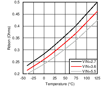
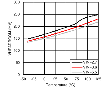
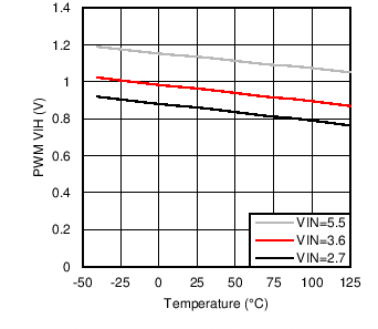 Figure 5. PWM VIH vs Temperature
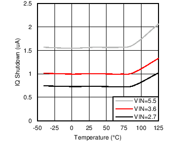
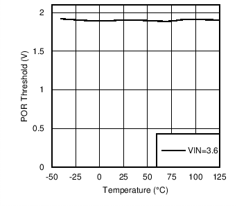
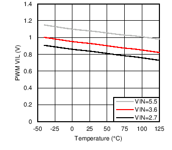 Figure 6. PWM VIL vs Temperature