SNAS425C October 2007 – October 2014 LM98519
PRODUCTION DATA.
- 1 Features
- 2 Applications
- 3 Description
- 4 Revision History
- 5 Pin Configuration and Functions
- 6 Specifications
-
7 Detailed Description
- 7.1 Overview
- 7.2 Functional Block Diagrams
- 7.3 Feature Description
- 7.4 Device Functional Modes
- 7.5 Programming
- 7.6 Register Maps
- 8 Application and Implementation
- 9 Power Supply Recommendations
- 10Layout
- 11Device and Documentation Support
- 12Mechanical, Packaging, and Orderable Information
Package Options
Mechanical Data (Package|Pins)
- PFC|80
Thermal pad, mechanical data (Package|Pins)
Orderable Information
7 Detailed Description
7.1 Overview
The LM98519 is a fully integrated, high performance 10-Bit, 65 MSPS signal processing solution for digital color copiers, scanners, and other image processing applications. High-speed signal throughput is achieved with an innovative six channel architecture utilizing Correlated Double Sampling (CDS), or Sample and Hold (SH) type sampling.
7.2 Functional Block Diagrams
 Figure 10. Channel Block Diagram
 Figure 11. Chip Block Diagram
7.3 Feature Description
7.3.1 Input Clamping and Biasing Circuitry
Many sensor input signals will be at a different common mode voltage than that of the LM98519 input circuitry. In these applications, AC coupling is used to block the DC voltage difference between the source and the AFE inputs. Input clamp circuits are used to set the AFE input at the proper common mode voltage.
Initial coarse clamping should be done using the PIB (Passive Input Bias) and/or AIB (Active Input Bias) circuitry. Setting the PIB enable bit connects 1-kΩ pull-up and pull-down resistors to the inputs to rapidly charge them to VDDA/2. Setting the AIB bit connects the VCLPEXT reference voltage to the inputs via low impedance switches. Either method will bring the input voltage very close to the desired level of VDDA/2.
The AIB and PIB must be disabled during normal operations.
During image capture, black level clamping is done by connecting the input pins to an internal reference voltage through a low impedance switch. The clamp is turned on periodically to correct any droop in the DC input voltage and minimize conversion errors.
The clamp switch will be turned on during the “Black” portion of the input signal when the input is at a known voltage level. The clamp will connect the inputs to a reference level of approximately 1.65 V. Optionally, a customer supplied reference voltage can be applied at the VCLPEXT pin. Clamp timing is controlled by the CLPIN input signal in combination with the register bit ANDen and the internal SAMPLE timing signal.
CLPIN can directly control the internal Clamp, or the combination of CLPIN and SAMPLE can be used. Clamping only during SAMPLE ensures that the input is clamped to the “Black” level rather than the average of “Black”, “Reset” and reset noise feed through signals.
 Figure 12. Input Protection and Clamping and Biasing Circuit
Input clamping happens in two stages as indicated by A and B in Figure 13:
(A) During initial system power up, the OVP clamp circuit should be enabled by register setting (Register 0x01, Bit 4 = 1). This provides a path for current to flow as the sensor is powered up, and the large common mode voltage output of the sensor reaches a steady state value. Once the sensor voltages have stabilized, the OVP circuit can be disabled. At this point the OS inputs will still be approximately 0.7 V above ground. Settling to 99% of final voltage will take approximately 18 ms for a 4.7-µF capacitance, assuming a 750-Ω diode/switch impedance.
(B) Then, the PIB and/or AIB circuits should be enabled to bring the OS inputs up to approximately VDDA/2 volts. After the OS voltages have charged to this level, the PIB and AIB biasing should be turned off. Settling to within 1mV of VDDA/2 will take approximately 18 ms for a 4.7-µF capacitance, assuming a 500-Ω charging resistance.
(C) During image acquisition, accurate DC clamping is provided by the CLPIN switch. This switch is enabled when the CLPIN input is asserted. In most applications, the Clamp Control bit (Register 0x02, Bit 0) should be set to gate the CLPIN signal with the internal sampling pulse. This will ensure that clamping is only done during the image portion of the optical black pixels. Settling to 1 mV for a 10 mV ΔV between the pedestal and black will take:
Smaller input capacitors will result in proportionally smaller settling times for all clamping modes.
7.3.2 Input Connections for 3 Channel Operation
For three channel only applications, the unused inputs should be connected with 10-kΩ resistors to VCLP_EXT to minimize noise coupling into the active inputs.
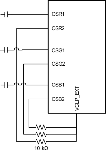 Figure 14. Input Connections for 3 Channel Operation
7.3.3 AFE References
A low noise reference structure is incorporated in the LM98519. Outputs (VREFTOUT approx. 2.23 V, VREFBOUT approx. 0.98V) and inputs (VREFTIN1, VREFTIN2, VREFBIN1, VREFBIN2) are provided to allow decoupling capacitors to be connected. VREFTOUT should be connected to VREFTIN1 and VREFTIN2. VREFBOUT should be connected to VREFBIN1 and VREFBIN2. Recommended capacitance is 1.0 µF between the top and bottom reference source, with 0.1 µF to AGND from both the top and bottom reference source. Connection and decoupling capacitor traces should all be as short as possible, and digital signals should be kept away from this area. Internal connections from VREFTOUT to VREFTIN1,2 and VREFBOUT to VREFBIN1,2 are present to reduce the impedance between outputs and inputs, but external connections should still be used for the best performance
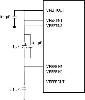 Figure 15. Reference Decoupling Example
7.3.4 Offset Control
Analog offset is provided before the ADC.
Two offset DACs are used to provide a coarse (CDAC) and fine (FDAC) offset that is applied prior to the CDS/SH stage.
- The offset CDAC (Coarse DAC) provides ±277 mV with ±4 bits of resolution in offset binary format.
- The offset FDAC (Fine DAC) provides ±111 mV (Large FDAC range) or ±60 mV (Small FDAC range) with ±10 bits of resolution in offset binary format. The FDAC range is controlled by the FDAC range bit for each color channel, in Register 0x03h, bits 3, 4, 5.
Table 1. Offset Binary Format
| CDAC (±4 bit) Offset Binary Format | FDAC (±10 bit) Offset Binary Format | |||||
|---|---|---|---|---|---|---|
| Hex. | Dec. | Offset Voltage (mV) | Hex. | Dec. | Offset Voltage (mV) | Offset Voltage (mV) |
| 1F | +15 | +277 | 7FF | +1023 | +111 | +60 |
| 11 | +1 | +18.5 | 401 | +1 | +0.109 | +0.059 |
| 10 | 0 | 0 | 400 | 0 | 0 | 0 |
| 0F | –1 | –18.5 | 3FF | –1 | –0.109 | –0.059 |
| 01 | –15 | –277 | 001 | –1023 | –111 | –60 |
| 00 | –16 | –277 | 000 | –1024 | –111 | –60 |
Table 2. CDAC Step Sizes
| CDS/SH+PGA Gain | CDAC LSB | ADC LSB |
|---|---|---|
| 1x | 1 | 15.7 |
| 10x | 1 | 157 |
| 20x | 1 | 314 |
Table 3. FDAC Step Sizes
| FDAC Range | CDS/SH+PGA Gain | FDAC LSB | ADC LSB |
|---|---|---|---|
| Small | 1x | 1 | 0.05 |
| Small | 10x | 1 | 0.50 |
| Small | 20x | 1 | 1.00 |
| Large | 1x | 1 | 0.09 |
| Large | 10x | 1 | 0.93 |
| Large | 20x | 1 | 1.8 |
7.3.5 Black Level Calibration (Offset)
Black level correction may be performed through one of two available methods: automatic or manual.
7.3.5.1 Manual Offset Adjustment
The manual method is intended for use with processing systems where the desired black level correction loop is external to the LM98519. In this mode the external processor controls the Black Level Offset registers.
Offset adjustment should be done using the average data from multiple Black pixels. The offset will be adjusted to set the Black pixel data as close as possible to the desired target value.
First the CDAC is adjusted until the error is reduced as much as possible given the CDAC step size for the current channel gain. (1 CDAC lsb = (15.7 to 314) ADC lsb depending on gain). Once the error is minimized with the CDAC, the FDAC is used to further converge the Black pixel data towards the target value.
After changing the channel gain, it may be desirable to repeat the offset adjustment.
7.3.5.2 Automatic Offset Adjustment
NOTE
During Automatic Offset Adjustment, the CDAC and FDAC register settings are Read Only.
During automatic black level calibration, the CDAC (coarse analog offset DAC) is used to bring the black level as close to the target as possible given the CDAC resolution.
Then the FDAC (Fine analog offset DAC) is applied to further converge the output to the desired black level target.
Two basic modes are available:
- CDAC and FDAC enabled – Used to converge to accurate Black target level as quickly as possible.
- FDAC Only mode – Used to maintain Black target level while avoiding large changes to offset. In FDAC only mode, the CDAC value is fixed, and the automatic adjustments only affect the FDAC.
CDAC and FDAC mode should be used to set the gain after power up and between scanning operations. FDAC Only mode should be used during scanning, to prevent large changes in offset from occurring in the image data. When using CDAC and FDAC mode, the value stored in Registers 0x25 and 0x26 is used to optimize trading of CDAC and FDAC steps. The default value is 321 decimal. To achieve the best trading, this value can be changed to 314 decimal. If the large FDAC range is enabled, this value should be changed to 184 decimal.
Use of the automatic mode involves enabling the black level offset auto-calibration bit in the black level clamp control register through the serial interface.
The ADC output value is averaged over the programmed number of pixels and subtracted from the desired black level code stored in the target black level register. The result of the subtraction may then be integrated by a preset scaling factor, effectively smoothing any sharp transitions present in the black level signal, before the resulting calculated offset is finally applied. The offset integration scaling factor is stored in the black level loop control register. The integration scaling values range from offset/2 to offset/128.
High Speed mode can be enabled to provide rapid initial convergence, with slower, more accurate convergence to the target value. High Speed mode is enabled by setting Register 0x23, Bit 1 = 1. The High Speed Mode offset integration value is set at Register 0x23, Bit 4. Two other parameters control the regions of operation around the target black value. The High Speed Mode Threshold and Hysteresis registers control the points where the transition from High Speed Mode to normal mode is made. When operating in High Speed Mode, the chip will transition to normal mode when Black Error < High Speed Threshold. When operating in Normal Mode, the chip will transition to High Speed Mode when Black Error > (High Speed Threshold + Hysteresis).
In automatic mode, the black level is determined from the ADC output during the Optical Black Pixels. The BLKCLP input pin is used to identify when the black pixels are being input to the IC. The rising edge of the BLKCLP input signal signals the beginning of the Optical Black Pixels. Alternatively, the Auto BLKCLP Pulse Generation (Register 0x23h, Bit 3) can be set to 1 to generate this signal internally. In that case, the BLKCLP pulse will begin 16 (6 channel mode) or 10 (3 channel mode) pixels after the falling edge of the CLPIN signal. Regardless of the source providing the BLKCLP start signal, the BLKCLP pulse duration is controlled by the Pixel Averaging setting in the BLKCLP_CTRL Register (0x24h, Bits 5:3).
NOTE
At high gain settings, it is possible that the Automatic Offset Adjustment may reach the full scale CDAC setting and fail to recover. In this case, the Automatic Offset Adjustment should be disabled, the CDAC and FDAC settings should be centered, and then the Automatic Offset Adjustment should be enabled.
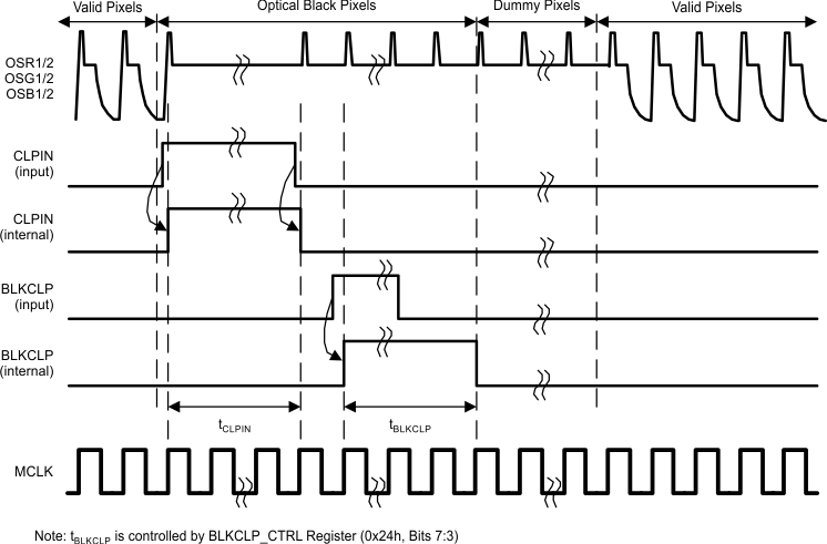 Figure 16. Black Calibration Timing – Manual BLKCLP
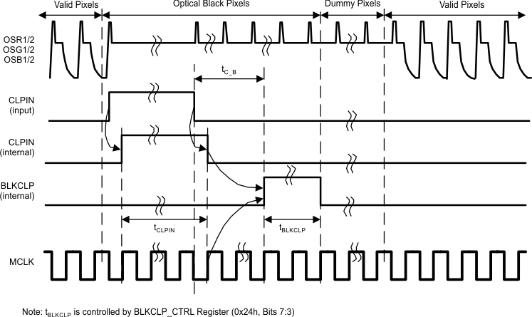 Figure 17. Black Calibration Timing – Automatic BLKCLP
7.3.5.3 Gain Control
The PGA provides a range from 1x to 10x gain with 8 bits of resolution. The gain curve is nominally:
where
- M is the 8-bit gain setting value from 0 to 255
In addition, the CDS/SH stage provides a 1x or 2.1x gain, giving an overall channel gain of 1x to 20x (0 dB to 26 dB).
7.3.5.4 White Level Calibration (AGC - Automatic Gain Control)
 Figure 19. White Level Calibration
During Automatic Gain Adjustment, the PGA and CDS/SH gain settings are Read Only.
The white calibration loop allows the LM98519 to automatically set the gain for the desired maximum ADC output. A digital input pin or configuration register bit is used to start the loop. This would normally be done once per page, or as needed for the particular system design. When triggered, the loop processes the output data during the defined white pixel range. The pixel range can be selected from a minimum of 1 pixel to a maximum of 65535 pixels. The starting pixel can be selected via the PK_DET_ST register at 0x2Ah, 0x2Bh and is referred to the rising edge of either the CLPIN or BLKCLP signal. The number of pixels is selected by the PK_DET_WID register at 0x2Ch, 0x2Dh.
During processing, a moving window average is performed. The size of the window is set by the PK_AVE register at 0x29, Bits 2:0. The window size is adjustable from 1 (no averaging) to 32 pixels. As each window average is calculated, the value is compared to the previous Peak White value (at the start of the line, the initial Peak White value is set to 0). If the new average is larger than the previous Peak White value, the Peak White value is replaced with the new average value. The window position is then incremented by 1 pixel and the process is repeated until the window average has processed all PK_DET_WID pixels.
If the AGC_ONB input is pulsed, the white calibration loop will operate for a fixed number of lines at the beginning of the scan. This duration is selected via the AGCDuration register at 0x2Eh. Valid settings are from 1 to 255 decimal. A duration setting of 0 will cause the loop to not run.
 Figure 20. AGC Loop
When the AGC_ONB input is pulsed, the register bit AGC_ON is set. The AGC_ON bit is cleared when the loop is terminated, which is when the number of lines allocated for the loop are exhausted. The AGC_ONB pin should be asserted for minimum of two pixels and should be deasserted before the loop is complete and the AGC_ON register bit is cleared.
Register 0x01, Bit 5 selects the polarity of the AGC_ONB input. The default is 0 for active low.
When the AGC loop begins operation, the AGC STATUS at Register 0x33, will be automatically cleared (as long as the serial interface mode bit at Register 0x01, Bit 3 is set to 1, MCLK present). At the end of the AGC loop operation, the AGC STATUS register can be read to check that the loop successfully converged for all channels. The status value should be 0x00 to indicate no Convergence Errors.
While the AGC loop is operating, a timing source is needed to provide a consistent reference point at the beginning of each line of pixels. Register 0x28, Bit 5 is used to select either the CLPIN or BLKCLP as the timing source. If Bit 5 = 0, the timing reference is the rising edge of CLPIN. If Bit 5 = 1, the timing reference is the rising edge of BLKCLP. The register setting PK_DET_ST selects the number of pixel after this timing reference that pixel averaging begins. The register setting PK_DET_WID selects the number of pixels after PK_DET_ST that are processed.
The purpose of the white loop is to find the correct gain setting so the brightest white pixels are at a specific ADC code target. The target value is set in the AGCTargetMSB and AGCTargetLSB registers. The target value is calculated from the register value as shown:
Table 4. AGC Target Values
| AGCTargetMSB (REGISTER 0x2F) |
AGCTargetLSB (REGISTER 0x30) |
AGC_TARG BINARY |
AGC_TARG DECIMAL |
|---|---|---|---|
| 11111111 | 1 | 1111111111 | 1023 |
| 11111111 | 0 | 1111111110 | 1022 |
| 10000000 | 1 | 1100000001 | 769 |
| 10000000 | 0 | 1100000000 | 768 |
| 00000000 | 1 | 1000000001 | 513 |
| 00000000 | 0 | 1000000000 | 512 |
7.3.6 Operating Mode Description
The white loop provides two different techniques for converging to the target value, Binary Search, and Incremental Search.
The Binary Search algorithm is intended to provide a rapid convergence to the target value. During initial operation, large changes in the channel gain are allowed. After each line, the allowed change is reduced significantly. For final convergence, the algorithm switches to the Incremental Search mode, to achieve low error.
The Incremental or Linear Search algorithm is intended to provide a low error, but will converge more slowly than the Binary method. The changes (if any) in channel gain are always done in 1 lsb increments to provide low overshoot and high accuracy of convergence.
7.4 Device Functional Modes
7.4.1 AFEPHASEn Details for SHP/SHD Input Mode
The SHP (sample reference) and SHD (sample signal) inputs are combined with the selected AFEPHASEn signal to generate the internal CLAMP and SAMPLE signals respectively. The SHP signal is ANDed with AFEPHASEn. The SHD signal is ANDed with the inverted AFEPHASEn signal.
The best performance will be achieved by selecting the AFEPHASEn timing that has the high period completely overlapping the SHP input timing, and the low period completely overlapping the SHD timing.
7.4.2 AFEPHASEn Details for SAMPLE and HOLD Input Mode
In Sample/Hold mode, the SAMPLE and HOLD inputs are used. The rising edge of SAMPLE defines the start of the sample control pulse, and the rising edge of HOLD defines the end of the sample control pulse. This sample control pulse is then gated by the low period of the AFEPHASEn signal to generate the resulting SAMPLE signal used internally.
The AFEPHASEn signal which has the low period overlapping the sample control pulse will give the best performance.
7.4.3 AFEPHASEn: 6 Channel and 3 Channel Modes
In 6 Channel Mode, there are two full cycles of MCLK and ADCCLK for each sensor pixel period. This allows the two AFE channels to be multiplexed into the single ADC. In this mode, there are 4 possible AFEPHASEn timings available.
In 3 Channel Mode, there is only one cycle of MCLK and ADCCLK per pixel period. Because of this, there are only 2 choices for AFEPHASEn, as shown in Figure 21 through Figure 23.
7.4.4 LM98519 AFEPHASE Synchronization
There are three main modes of operation for the LM98519
- 6 channel mode using ADC Rate MCLK – Clock Doubler is bypassed
- 6 channel mode using Pixel Rate MCLK – Clock Doubler is used
- 3 channel mode using Pixel Rate MCLK – Clock Doubler is bypassed
In case #1, where an ADC rate (2x of pixel rate) clock is input, the LM98519 needs one additional signal to ensure synchronization between the internal sampling phases and the pixel rate input signal.
This synchronization is done using the CLPIN input signal in combination with MCLK. The CLPIN input generates an internal reset signal that sets the internal AFEPHASE state machine into a known relationship with MCLK and CLPIN. This ensures the AFEPHASE sampling is synchronized to the host sensor timing.
Figure 21 through Figure 23 indicate the phase relationship between MCLK and AFEPHASE when CLPIN is used for synchronization.
 Figure 21. 6 Channel Mode – ADC Rate MCLK
7.4.5 Sampling Timing Diagrams
NOTE
4 (6 Channel Mode) or 2 (3 Channel Mode) AFEPHASE settings are available to provide flexibility of sample timing.
For ease of use, AFEPHASE = 11 is the default setting in 6 channel mode, and AFEPHASE = X1 is the default setting for 3 channel mode, as shown in select diagrams. Specified values for these timings are measured at AFEPHASE = 11. For other AFEPHASE settings,these sample input timings will shift earlier with respect to MCLK as follows:
- AFEPHASE = 10 – Earlier by ¼ pixel period
- AFEPHASE = 01 – Earlier by ½ pixel period
- AFEPHASE = 00 – Earlier by ¾ pixel period
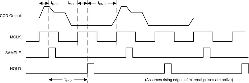 Figure 24. SH3 Timing Mode – ADC Rate Clock Input (Pixel Rate MCLK not Supported in SH3)
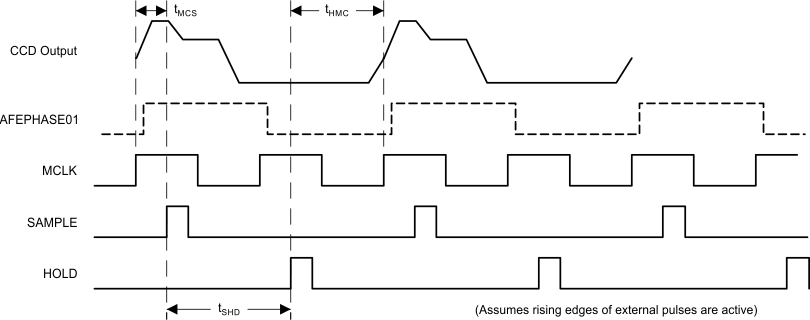 Figure 25. SH2 Timing Mode – ADC Rate Clock Input
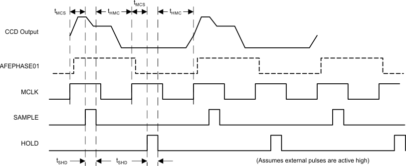 Figure 27. SH1b/CDSb Timing Mode – ADC Rate Clock Input
7.5 Programming
7.5.1 Using Black Pixel Average
In most applications, the Black Pixel Average bit should be set.
During loop operation, the ADC_MAX or average maximum ADC value is found during the white pixels. The Black Pixel Average value is then subtracted from this ADC_MAX value to find the present white value. This ADC_WHT value is then used for comparison to the target white pixel value TARG_WHT. This is done to eliminate the effects that changes in the system gain will have on the Black Pixel Average value. As gain is increased or decreased, the previously calibrated Black Pixel Average value will change also. When the white loop operation is complete, the gain is set to provide the proper white level referenced to the Black Pixel Average value. Then the Black Loop will be run once more to set the Black Pixel Average at the desired level, and the White level will still be calibrated to the proper level.
In addition, the following registers should be initialized before starting the loop:
Table 5. Initialize Registers Before Loop
| REGISTER | FUNCTION |
|---|---|
| PK_DET_ST (0x2Ah, 0x2Bh) |
Start of the white pixel averaging in pixels from rising edge of CLPIN or BLKCLP |
| PK_DET_WID (0x2Ch, 0x2Dh) |
Number of pixels in each line over which white pixels are averaged |
| AGCDuration (0x2Eh) |
Duration in number of lines the loop should run. If set to 0, the loop will not run. Valid settings are 1 to 255. |
| AGCTarget (0x2Fh, 0x30h) |
AGC target, between 512 to 1023 |
| AGCTolerance (0x31h) |
Allowed error margin from the target value |
| AGC_BLKINT (0x32h) |
Black Offset Integration, if used |
| AGC_CONFIG (0x28h) |
Select reference edge CLPIN or BLKCLP rising edge, Enable/Disable AGC_ONB Pin, Incremental Search Enable, Black Offset Enable |
After all registers are initialized, the AGC_ON bit (0x28h, b0) can be set, or the AGC_ONB pin can be pulsed to start the white loop.
7.5.2 Sample Timing Control
Sample timing is controlled through the combination of the selected internal AFEPHASEn signal, and one or several user inputs.
The input timing control pins can operate in two different modes:
SAMPLE and HOLD (Used with S/H mode sampling only)
In this mode, the rising edge of the SAMPLE signal controls the start of the sampling, while the rising edge of HOLD stops sampling and holds the signal. This mode cannot be used with CDS operation.
SHP and SHD (Used with CDS and S/H modes of sampling)
In this mode, the SHP pulse is used to sample the reference level of the signal, while the SHD pulse is used to sample the signal (brightness) information when CDS mode is used. If CDS is turned off, then SHD is used to control the signal sample timing and SHP is not used.
The different input timing modes are selected by bits in Registers 0x00, 0x02, and 0x04, as shown in Table 6:
Table 6. Input Timing Modes
| MODE | REG 0x04[1] |
REG 0x02[7] |
REG 0x02[3:2] |
REG 0x02[1] |
REG 0x00[0] |
DESCRIPTION |
|---|---|---|---|---|---|---|
| SH3 (Default) | 0 | 1 | See(3) | 0 | 0 | Sample and Hold mode, clocked by SAMPLE and HOLD clocks(2) |
| SH2 | 1 | 1 | 0 | 0 | Sample and Hold mode, clocked by SAMPLE and HOLD clocks(1) | |
| SH1a | 1 | 0 | 1 | 0 | Sample and Hold mode, clocked by AFEPHASE(1) | |
| SH1b | 1 | 1 | 1 | 0 | Sample and Hold mode, clocked by SHD(1) | |
| CDSa | 1 | 0 | 1 | 1 | CDS mode, sampled by AFEPHASE(1) | |
| CDSb | 1 | 1 | 1 | 1 | CDS mode, sampled by SHP and SHD clocks(1) |
In modes SH1a and CDSa, the internal Sample or Clamp and Sample timing signals are generated from the selected AFEPHASEn signal.
In modes SH1b and CDSb, the input SHD or SHD and SHP signals are ‘gated’ by the internal AFEPHASEn signal to create the internal Sample and Clamp signals.
In mode SH2, the SAMPLE and HOLD timing signals are directly input to the sampling stage of the AFE. Subsequent stages are still clocked by the selected AFEPHASEn and MCLK.
In mode SH3, the SAMPLE and HOLD timing signals are directly input to the sampling stage of the AFE, and are also used to set the internal AFEPHASE timing for subsequent stages. In this mode, CLPIN is not required to set the AFEPHASE timing. SH3 mode only supports ADC Rate MCLK.
Please refer to the timing diagrams in Figure 21 through Figure 23 to see the relationship between the sample timing inputs and the internal AFEPHASEn signal.
7.5.3 Timing Monitor Outputs
In timing monitor mode, the internal CLAMP and SAMPLE (CDS Mode) or SAMPLE (S/H Mode) timing signals are output on the DR[3:2] pins. This enables easy confirmation of the actual internal timing configuration. Timing monitor mode is enabled by setting Register 0x00, Bit 1 = 1.
Table 7 describes the signals present on the DR[2] and DR[3] outputs in the different timing modes:
Table 7. Signal Presets
| SAMPLE MODE | DR[2] | DR[3] |
|---|---|---|
| SH2, SH3 | SH Sample Signal | PGA Sample B (active low) |
| SH1a, SH1b | SH Sample Signal | SH Sample Signal |
| CDSa, CDSb | Sample Signal Level | Sample Reference Level |
7.5.4 Output Data Test Pattern Generation
Special test patterns will be generated to help in testing data processing. Four basic types of waveform can be generated and they are:
- Fixed Pattern
- Horizontal Gradation Pattern (main scan)
- Vertical Gradation Pattern (sub-scan)
- Lattice Pattern
Table 8. Register Definitions for Test Pattern Parameters
| REGISTER | DEFINITION | |||
|---|---|---|---|---|
| PK_DET_ST | This register defines the start of the Valid Pixel region from the rising edge of CLMPIN or BLKCLP, in Pixels. | |||
| PK_DET_WID | This register defines the duration (pixels) of the Valid Pixel region. | |||
| PATSW | Enable/Disable test pattern output. | |||
| PATMODE | Sets which test pattern mode is used:
|
|||
| PATREGSEL | Test pattern can be initiated on a single color or all three colors at the same time. When only one color is selected, the other colors are set to maximum 1023 code.
|
|||
| TESTPLVL | Output code 0 to 1023. In Fixed Pattern it is code output during the Valid Pixel range. During Horizontal Gradation and Vertical Gradation it is used as the initial code. In Lattice Pattern it is the level during the Valid Pixel range except for the first pixel every PATW pixels in the horizontal range and for first line every PATW lines. | |||
| PATW | Gradation pitch, this is interval at which the pattern Code Step provided in PATS register is applied. | |||
| PATS | Pattern Code Step, this contains the code step increment applied every PATW interval. | |||
| LINE_INT | Test pattern output delay. This defines the delays in number of lines between Red to Green and Green to Blue. This sequence is fixed, R->G->B, and when this register is 0, all colors switch simultaneously. This delay is used only on the initial start and the sequence of colors is fixed. | |||
7.5.5 Fixed Pattern
Outputs fixed code in the TESTPLVL register during Valid Pixel range.
7.5.6 Horizontal Gradation
Code in the TESTPLVL is outputted initially in the PATW pixels of the Valid Pixel region, and then code is incremented by PATS value every PATW pixels for the rest of the active region. If the code reaches the maximum (less than or equal to 1023), it is reset to the initial value in TESTPLVL and pattern repeated. Same sequence is repeated for the all the lines.
7.5.7 Vertical Gradation
Code in the TESTPLVL is outputted initially in the first PATW lines of the scan and fixed for all of the Valid Pixel region, and then the code is incremented by PATS value every PATW lines and the new code is applied during active region till the next increment. This is repeated till code reaches the maximum (less than or equal to 1023) then the code is reset to the initial value and the sequence repeated.
7.5.8 Lattice Pattern
This is combination of Horizontal and Vertical Gradation pattern. Here the register PATW defines interval in pixels for horizontal scan and in lines for the vertical scan. At start of the test the output is set to PATS level for the whole first line and every line at PATW interval. In rest of the lines of the output goes to PATS for the first pixel then goes TESTPLVL for PATW-1 pixels, then goes back to PATS for one pixel and then to TESTPLVL for PATW-1 pixels, the cycle repeats till the end of line.
All test pattern generation continues once initiated by setting of PATSW till it is reset.
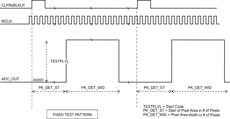 Figure 29. Fixed Test Pattern
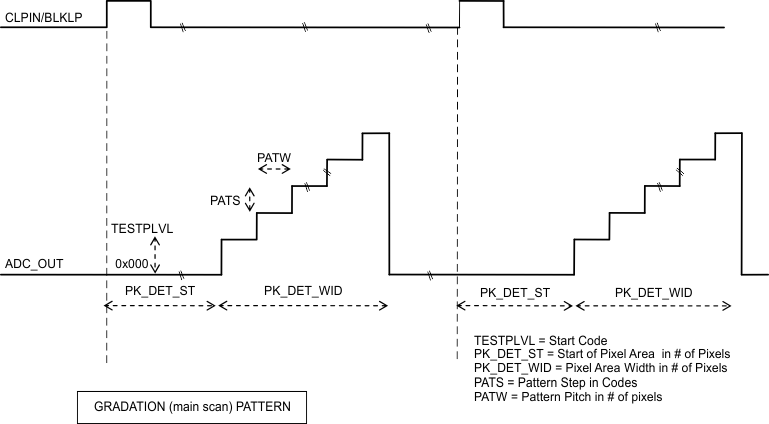 Figure 30. Gradation (Main Scan) Pattern
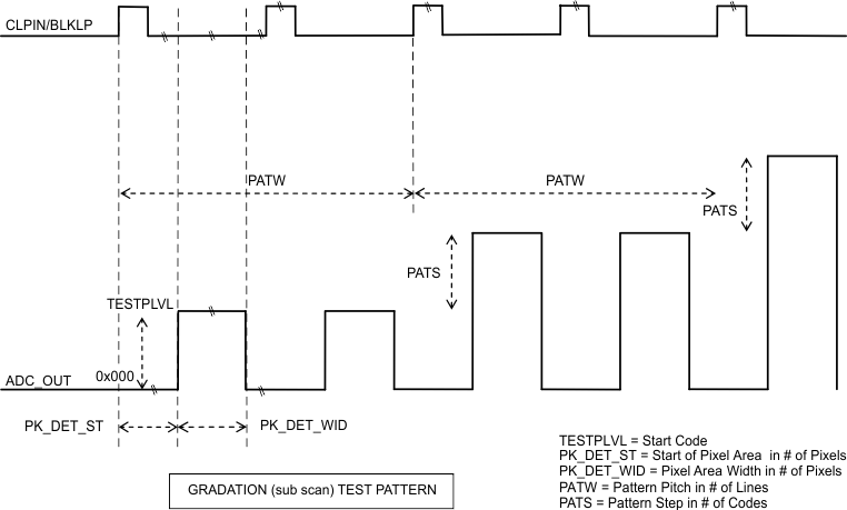 Figure 31. Gradation (Sub Scan) Test Pattern
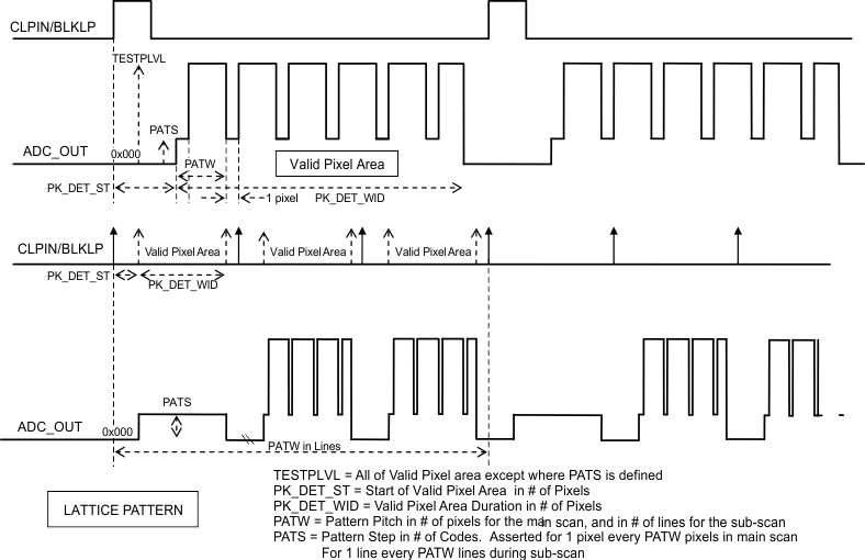 Figure 32. Lattice Pattern
7.5.9 Serial Interface
The serial control interface is based on the common microwire interface with a few specific timing details, as shown below. Bits A5, A4, A3, A2, A1, A0 select the configuration register currently being written to or read within the flat register space.
NOTE
The serial interface is initially configured to work in the absence of MCLK. Once MCLK is established, the configuration can be changed to work with MCLK. This is done by setting the Serial Interface Mode bit in Register 0x01, bit 3 = 1. Operation with MCLK will reduce any timing restrictions required in the non-MCLK mode. In addition, the Auto Clear of AGC Status will only work in MCLK Present mode.
7.5.10 Serial Write
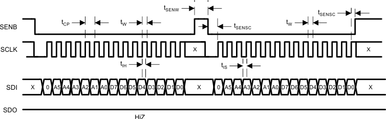 Figure 33. Serial Write
- The positive edge of SCLK is used to receive data on SDI.
- Last 15 bits of data before SEN toggled high will be loaded into AFE.
- A command whose length is less than 15 bits will be discarded.
- SDO will be Hi-Z during write operation.
- At the second cycle shown above, either read or write command is possible.
- The MODE bit must be “0” when writing to registers.
- A Write command consists of one MODE bit, 6 address bits and 8 data bits.
- While SEN is high, the AFE will accept either high or low with respect to SCLK and SDI.
7.5.11 Serial Read
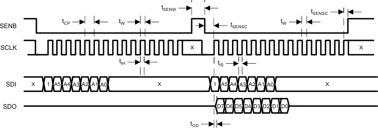 Figure 34. Serial Read
- The positive edge of SCLK is used to receive data on SDI.
- Last 15 bits of data before SEN goes high will be loaded.
- Command whose length is less than 15 bits will be discarded.
- Readout data will appear on SDO at the second cycle above.
- The readout data is clocked at the positive edge of SCLK.
- SDO is Hi-Z except when read out data appears on SDO.
- At the second cycle shown above, either read or write command is possible.
- The MODE bit must be “1” when reading from registers.
- A Read command will contain one MODE bit, 6 address bits, and 8 dummy data bits which are ignored.
- While SEN is high, the AFE will accept either high or low with respect to SCLK and SDI.
7.6 Register Maps
7.6.1 Configuration Registers
Table 9. Register Summary
| HEX ADDRESS (A5-A0) |
REGISTER NAME | COMMENTS |
|---|---|---|
| 0x00 to 0x06 | Configuration 0 to 6 | Configuration settings |
| 0x07 | Device Revision | |
| 0x08 | GA_R1 | OS_R1 Channel Gain and Offset Registers (CDS / SH Gain is NOT located here) |
| 0x09 | C_OFFS_R1 | |
| 0x0A | F_OFFS_R1_MSB | |
| 0x0B | F_OFFS_R1_LSB | |
| 0x0C | GA_R2 | OS_R2 Channel Gain and Offset Registers |
| 0x0D | C_OFFS_R2 | |
| 0x0E | F_OFFS_R2_MSB | |
| 0x0F | F_OFFS_R2_LSB | |
| 0x10 to 0x13 | OS_G1 Channel Gain and Offset Registers | |
| 0x14 to 0x17 | OS_G2 Channel Gain and Offset Registers | |
| 0x18 to 0x1B | OS_B1 Channel Gain and Offset Registers | |
| 0x1C to 0x1F | OS_B2 Channel Gain and Offset Registers | |
| 0x20 | TARG_BLK_R | |
| 0x21 | TARG_BLK_G | |
| 0x22 | TARG_BLK_B | |
| 0x23 | Black Level Loop Control | |
| 0x24 | Black Level Loop Settings | |
| 0x25 | CDAC Threshold for BLK LP MSB | |
| 0x25 | CDAC Threshold for BLK LP LSB | |
| 0x27 | Fast Mode | |
| 0x28 | White Level Loop Control | |
| 0x29 | PK_AVG | |
| 0x2A | PK_DET_ST_MSB | |
| 0x2B | PK_DET_ST_LSB | |
| 0x2C | PK_DET_WID_MSB | |
| 0x2D | PK_DET_WID_LSB | |
| 0x2E | AGCDuration | |
| 0x2F | AGCTargetMSB | |
| 0x30 | AGCTargetLSB | |
| 0x31 | AGCTolerance | |
| 0x32 | AGC_BLKINT | |
| 0x33 | AGC STATUS | |
| 0x34 to 0x37 | TBD | |
| 0x38 | Test Pattern Mode | |
| 0x39 | Test Pattern Settings 1 | |
| 0x3A | Test Pattern Settings 2 | |
| 0x3B | PATW | |
| 0x3C | PATS | |
| 0x3D | LINE_INTVL | |
| 0x3E | Reserved | |
| 0x3F | Reserved |
7.6.2 Configuration Register Details
Table 10. Configuration Registers Details
| ADDR (HEX) |
REGISTER NAME |
DEFAULT (HEX) |
DESCRIPTION |
|---|---|---|---|
| 0x00 - 0x07 CONFIGURATION REGISTERS | |||
| 0x00 | ANLG_CONFG | 0x28 | Main Configuration
|
| 0x01 | INTF_CONFG | 0x10 | Interface Configuration
|
| 0x02 | CLP_CONFG Sample Timing Control |
0x9C | Clamp Control
|
| 0x03 | CDSG_CONFIG CDS / SH Gain Enable FDAC Range Select |
0x00 | FDAC Range, CDS Gain Selection
|
| 0x04 | Main Configuration 4 | 0x00 |
|
| 0x05 | Main Configuration 5 | 0x77 |
|
| 0x06 | SRESET | 0x00 | Soft Reset
|
| 0x07 | Device Revision | 0x10 | Read Only This number reflects the device revision and updated every time any major or minor change is made to the silicon. |
| 0x08 – 0x0F Red CHANNEL PGA GAIN, CDAC and FDAC OFFSETS | |||
| 0x08 | GA_R1 | 0x00 |
|
| 0x09 | C_OFFS_R1 | 0x10 |
|
| 0x0A | F_OFFS_R1 | 0x80 |
|
| 0x0B | F_OFFS_R1 LSB | 0x00 |
|
| 0x0C | GA_R2 | 0x00 |
|
| 0x0D | C_OFFS_R2 | 0x10 |
|
| 0x0E | F_OFFS_R2 | 0x80 |
|
| 0x0F | F_OFFS_R2 LSB | 0x00 |
|
| 0x10 – 0x17 GREEN CHANNEL PGA GAIN, CDAC and FDAC OFFSETS | |||
| 0x10 | GA_G1 | 0x00 |
|
| 0x11 | C_OFFS_G1 | 0x10 |
|
| 0x12 | F_OFFS_G1 | 0x80 |
|
| 0x13 | F_OFFS_G1 LSB | 0x00 |
|
| 0x14 | GA_G2 | 0x00 |
|
| 0x15 | C_OFFS_G2 | 0x10 |
|
| 0x16 | F_OFFS_G2 | 0x80 |
|
| 0x17 | F_OFFS_G2 LSB | 0x00 |
|
| 0x18 – 0x1F BLUE CHANNEL PGA GAIN, CDAC and FDAC OFFSETS | |||
| 0x18 | GA_B1 | 0x00 |
|
| 0x19 | C_OFFS_B1 | 0x10 |
|
| 0x1A | F_OFFS_B1 | 0x80 |
|
| 0x1B | F_OFFS_B1 LSB | 0x00 |
|
| 0x1C | GA_B2 | 0x00 |
|
| 0x1D | C_OFFS_B2 | 0x10 |
|
| 0x1E | F_OFFS_B2 | 0x80 |
|
| 0x1F | F_OFFS_B2 LSB | 0x00 |
|
| 0x20 - 0x27 BLACK LEVEL OFFSET CALIBRATION REGISTERS | |||
| 0x20 | TARG_BLK_R | 0x20 |
|
| 0x21 | TARG_BLK_G | 0x20 |
|
| 0x22 | TARG_BLK_B | 0x20 |
|
| 0x23 | BLKCLP_CTL0 | 0x0C | Black Level Loop Control
|
| 0x24 | BLKCLP_CTRL1 | 0x84 | Digital Black Level Clamp Control
|
| 0x25 | CDAC_THLD_MSB | 0x50 | CDAC Threshold for BLK LP MSB Default value is 321d, so loop will change FDAC by 321 to compensate for change of 1 in CDAC. To optimize even further, this can be changed to 314d. If FDAC is set to the large range, then this value should be changed to 184d.
|
| 0x26 | CDAC_THLD_LSB | 0x40 | CDAC Threshold for BLK LP LSB
|
| 0x27 | High Speed Mode | 0x88 |
|
| 0x28 – 0x37 WHITE LEVEL GAIN CALIBRATION REGISTERS | |||
| 0x28 | AGC_CONFG | 0x00 |
|
| 0x29 | PK_AVE | 0x04 | Number of pixels in running average during white calibration loop
|
| 0x2A | PK_DET_ST_MSB | 0x00 | Starting pixel for peak detection. 16 bit value. Number of pixels after rising edge trigger event. (CLPIN or BLKCLP) (0 to 65535) |
| 0x2B | PK_DET_ST_LSB | 0x00 | |
| 0x2C | PK_DET_WID_MSB | 0x00 | Duration of peak detection after PK_DET_ST. 16 bit value (0 to 65535) |
| 0x2D | PK_DET_WID_LSB | 0x00 | |
| 0x2E | AGCDuration | 0x10 |
|
| 0x2F | AGCTargetMSB | 0xE0 |
|
| 0x30 | AGCTargetLSB | 0x00 |
|
| 0x31 | AGCTolerance | 0x28 |
|
| 0x32 | AGC_BLKINT | 0x00 | AGC Offset Integration
|
| 0x33 | AGC STATUS | 0x00 | AGC Status – Read Only
|
| 0x34 | Reserved | 0x32 | Must be kept with Power-on-default values. |
| 0x35 | Reserved | 0x54 | Must be kept with Power-on-default values. |
| 0x36 | Reserved | 0x00 | Must be kept with Power-on-default values. |
| 0x37 | Reserved | 0x00 | Must be kept with Power-on-default values. |
| 0X38 to 0X3F USER TEST PATTERNS REGISTERS | |||
| 0x38 | TEST_PAT_CTL | 0x00 | Test Pattern Mode
|
| 0x39 | TESTPLVL_MSB | 0x00 |
|
| 0x3A | TESTPLVL_LSB | 0x00 |
|
| 0x3B | PATW | 0x00 |
|
| 0x3C | PATS | 0x00 |
|
| 0x3D | LINE_INTVL | 0x00 |
|
| 0x3E | Reserved | ||
| 0x3F | Reserved | ||