SNAS425C October 2007 – October 2014 LM98519
PRODUCTION DATA.
- 1 Features
- 2 Applications
- 3 Description
- 4 Revision History
- 5 Pin Configuration and Functions
- 6 Specifications
-
7 Detailed Description
- 7.1 Overview
- 7.2 Functional Block Diagrams
- 7.3 Feature Description
- 7.4 Device Functional Modes
- 7.5 Programming
- 7.6 Register Maps
- 8 Application and Implementation
- 9 Power Supply Recommendations
- 10Layout
- 11Device and Documentation Support
- 12Mechanical, Packaging, and Orderable Information
Package Options
Mechanical Data (Package|Pins)
- PFC|80
Thermal pad, mechanical data (Package|Pins)
Orderable Information
5 Pin Configuration and Functions
80-Pin
PFC Package
(Top View)
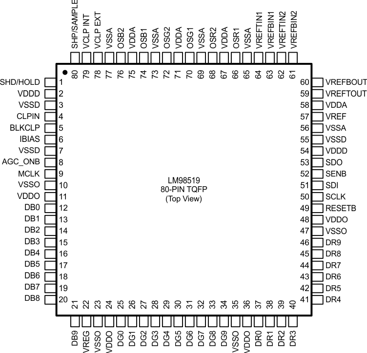
Pin Functions(1)
| PIN | TYPE | DESCRIPTION | |
|---|---|---|---|
| NUMBER | NAME | ||
| 1 | SHD/ HOLD | DI | Data Clamp Pulse |
| 2, 54 | VDDD | PI | Digital Power Supply |
| 3, 7, 55 | VSSD | PI | Digital Power Supply Ground |
| 4 | CLPIN | DI | Input Pulse That Invokes an Input Clamp Switch |
| 5 | BLKCLP | DI | Input Pulse that Invokes a Black Clamp Calibration Loop Pulldown 108kΩ |
| 6 | IBIAS | AO | Optional IBIAS resistor connection. To minimize device to device power consumption variation, connect an 11k Ohm 1% resistor to VSSA. If no resistor is used, the internal bias and power supply currents will be subject to normal device to device variation. |
| 8 | AGC_ONB | DI | Input Pulse that Invokes the White Calibration Loop. Tie high to disable White Clamp. Pulse Low to initiate White Clamp. (Active Low) Pulldown 108kΩ |
| 9 | MCLK | DI | Master Clock Input |
| 10, 23, 35, 47 | VSSO | PI | Output Driver Power Supply Ground |
| 11, 24, 36, 48 | VDDO | PI | Output Driver Power Supply |
| 12-21 | DB0–DB9 | DO | Bit 0 – Bit 9 of the Blue Channel |
| 22 | VREG | PO | Decoupling connection for VREG – Internal Voltage for Logic |
| 25-34 | DG0–DG9 | DO | Bit 0 – Bit 9 of the Green Channel |
| 37-46 | DR0–DG9 | DO | Bit 0 – Bit 9 of the Red Channel |
| 39 | DR2 (TESTO0) | DO | Bit 2 of Red Channel Data or TESTO0 timing monitor output (Timing monitor output selected by setting Register 0x00, Bit 1 = 1) |
| 40 | DR3 (TESTO1) | DO | Bit 3 of Red Channel Data or TESTO1 timing monitor output (Timing monitor output selected by setting Register 0x00, Bit 1 = 1) |
| 49 | RESETB | DI | Master Reset Input (Active Low) Pulldown 108 kΩ |
| 50 | SCLK | DI | Serial Clock for the 4-wire Serial Interface |
| 51 | SDI | DI | Serial Input Data for the 4-wire Serial Interface |
| 52 | SENB | DI | Serial Enable (Active Low) for the 4-wire Serial Interface Pulldown 108 kΩ |
| 53 | SDO | DO | Serial Output Data for the 4-wire Serial Interface |
| 56, 65, 69, 73, 77 | VSSA | PI | Analog Power Supply Ground |
| 57 | VREF | AO | Reference Voltage Bypass |
| 58, 67, 71, 75 | VDDA | PI | Analog Power Supply |
| 59 | VREFTOUT | AO | Top Reference Bypass. Connect to bypass capacitors (see applications section) and VREFTINx. – Approx. 2.23 V output(2) |
| 60 | VREFBOUT | AO | Bottom Reference Bypass. Connect to bypass capacitors (see applications section) and VREFBINx. – Approx. 0.98 V output(2) |
| 61 | VREFBIN2 | AI | Bottom Reference Input Voltage for the ADC. Connect to VREFBOUT. |
| 62 | VREFTIN2 | AI | Top Reference Input Voltage for the ADC. Connect to VREFTOUT. |
| 63 | VREFBIN1 | AI | Bottom Reference Input Voltage for the AFE. Connect to VREFBOUT. |
| 64 | VREFTIN1 | AI | Top Reference Input Voltage for the AFE. Connect to VREFTOUT. |
| 66 | OSR1 | AI | Input Voltage 1 for the Red Channel |
| 68 | OSR2 | AI | Input Voltage 2 for the Red Channel |
| 70 | OSG1 | AI | Input Voltage 1 for the Green Channel |
| 72 | OSG2 | AI | Input Voltage 2 for the Green Channel |
| 74 | OSB1 | AI | Input Voltage 1 for the Blue Channel |
| 76 | OSB2 | AI | Input Voltage 2 for the Blue Channel |
| 78 | VCLP_EXT | AI | External Clamp Voltage |
| 79 | VCLP_INT | AO | Internally Supplied V-Clamp Voltage |
| 80 | SHP/ SAMPLE | DI | Pedestal Clamp Pulse |
(1) A – Analog, D – Digital, P – Power, I – Input, O – Output, PD – Pull-down resistor to VSSD, PU – Pull-up resistor to VDDD
(2) Voltages provided for debugging only. Not an ensured specification.