SNOS674I October 1997 – February 2024 LMC6482 , LMC6484
PRODUCTION DATA
- 1
- 1 Features
- 2 Applications
- 3 Description
- 4 Pin Configuration and Functions
- 5 Specifications
- 6 Detailed Description
- 7 Application and Implementation
- 8 Device and Documentation Support
- 9 Revision History
- 10Mechanical, Packaging, and Orderable Information
Package Options
Refer to the PDF data sheet for device specific package drawings
Mechanical Data (Package|Pins)
- D|14
- N|14
Thermal pad, mechanical data (Package|Pins)
Orderable Information
7.2.2 Typical Single-Supply Applications
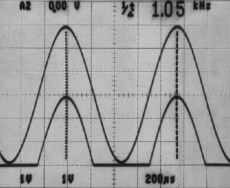
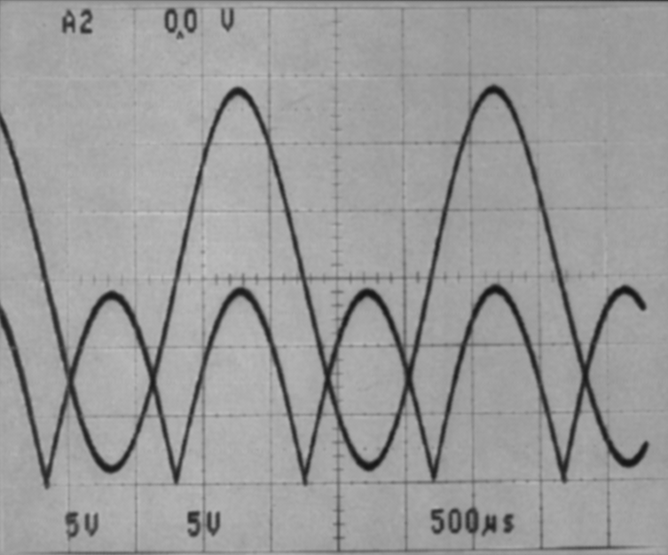
The circuit in Figure 7-17 uses a single supply to half-wave rectify a sinusoid centered about ground. Ri limits current into the amplifier caused by the input voltage exceeding the supply voltage. Full-wave rectification is provided by the circuit in Figure 7-19.
 Figure 7-17 Half-Wave Rectifier With
Input Current Protection (Ri)
 Figure 7-18 Half-Wave Rectifier
Waveform
Figure 7-18 Half-Wave Rectifier
WaveformIn Figure 7-23, dielectric absorption and leakage is minimized by using a polystyrene or polyethylene hold capacitor. The droop rate is primarily determined by the value of CHOLD and diode leakage current. The ultra-low input current of the LMC648x has a negligible effect on droop. For applications requiring ultra-low input bias current, see the OPA928.
 Figure 7-19 Full-Wave Rectifier With
Input Current Protection (RI)
 Figure 7-21 Large Compliance Range
Current Source
 Figure 7-23 Low-Voltage Peak Detector
With Rail-To-Rail Peak Capture Range
 Figure 7-20 Full-Wave Rectifier
Waveform
 Figure 7-22 Positive Supply Current
Sense
Figure 7-22 Positive Supply Current
SenseThe high CMRR (82dB) of the LMC648x allows excellent accuracy throughout the rail-to-rail dynamic capture range of the circuit.
 Figure 7-24 Rail-to-Rail Sample and
Hold
Figure 7-24 Rail-to-Rail Sample and
HoldThe low-pass filter circuit in Figure 7-25 can be used as an anti-aliasing filter with the same voltage supply as the A/D converter.
Filter designs can also take advantage of the LMC648x ultra-low input current. The ultra-low input current yields negligible offset error even when large value resistors are used. This in turn allows the use of smaller valued capacitors that take less board space and cost less.
 Figure 7-25 Rail-to-Rail, Single-Supply
Low-Pass Filter