SNOS956E June 2001 – August 2014 LMH6654 , LMH6655
PRODUCTION DATA.
- 1 Features
- 2 Applications
- 3 Description
- 4 Revision History
- 5 Pin Configuration and Functions
- 6 Specifications
- 7 Application and Implementation
- 8 Power Supply Recommendations
- 9 Layout
- 10Device and Documentation Support
- 11Mechanical, Packaging, and Orderable Information
Package Options
Mechanical Data (Package|Pins)
Thermal pad, mechanical data (Package|Pins)
Orderable Information
6 Specifications
6.1 Absolute Maximum Ratings
over operating free-air temperature range (unless otherwise noted)(1)| MIN | MAX | UNIT | ||
|---|---|---|---|---|
| VIN Differential | ±1.2 | V | ||
| Output Short Circuit Duration | See (3) | |||
| Supply Voltage (V+ − V−) | 13.2 | V | ||
| Voltage at Input pins | V+ +0.5 V- -0.5 |
V | ||
| Junction Temperature(4) | 150 | °C | ||
| Soldering Information | Infrared or Convection (20 sec.) | 235 | °C | |
| Wave Soldering (10 sec.) | 260 | °C | ||
(1) Stresses beyond those listed under Absolute Maximum Ratings may cause permanent damage to the device. These are stress ratings only, which do not imply functional operation of the device at these or any other conditions beyond those indicated under Recommended Operating Conditions. Exposure to absolute-maximum-rated conditions for extended periods may affect device reliability.
6.2 Handling Ratings
| MIN | MAX | UNIT | |||
|---|---|---|---|---|---|
| Tstg | Storage temperature range | −65 | 150 | °C | |
| V(ESD) | Electrostatic discharge(2) | Human body model (HBM), per ANSI/ESDA/JEDEC JS-001, all pins(1) |
2000 | V | |
| Machine model (MM)(2) | 200 | ||||
(1) JEDEC document JEP155 states that 2000-V HBM allows safe manufacturing with a standard ESD control process.
(2) JEDEC document JEP157 states that 200-V MM allows safe manufacturing with a standard ESD control process.
6.3 Recommended Operating Conditions(1)
over operating free-air temperature range (unless otherwise noted)| MIN | NOM | MAX | UNIT | ||
|---|---|---|---|---|---|
| Supply Voltage (V+ - V−) | ±2.5 | ±6.0 | V | ||
| Operating Temperature Range | −40 | 85 | °C | ||
6.4 Thermal Information
| THERMAL METRIC(1) | SOIC (D) | VSSOP (DGK) | SOT-23 (D) | UNIT | |
|---|---|---|---|---|---|
| 8 PINS | 8 PINS | 5 PINS | |||
| RθJA | Junction-to-ambient thermal resistance | 172 | 235 | 265 | °C/W |
(1) For more information about traditional and new thermal metrics, see the IC Package Thermal Metrics application report, SPRA953.
±5V Electrical Characteristics
Unless otherwise specified, all limits ensured for V+ = +5V, V− = −5V, VCM = 0V, AV = +1, RF = 25Ω for gain = +1, RF = 402Ω for gain ≥ +2, and RL = 100Ω. Boldface limits apply at the temperature extremes.| PARAMETER | TEST CONDITIONS | MIN(6) | TYP(5) | MAX(6) | UNIT | |
|---|---|---|---|---|---|---|
| DYNAMIC PERFORMANCE | ||||||
| fCL | Close Loop Bandwidth | AV = +1 | 250 | MHz | ||
| AV = +2 | 130 | |||||
| AV = +5 | 52 | |||||
| AV = +10 | 26 | |||||
| GBWP | Gain Bandwidth Product | AV ≥ +5 | 260 | MHz | ||
| Bandwidth for 0.1 dB Flatness | AV +1 | 18 | MHz | |||
| φm | Phase Margin | 50 | deg | |||
| SR | Slew Rate (8) | AV = +1, VIN = 2 VPP | 200 | V/µs | ||
| tS | Settling Time 0.01% |
AV = +1, 2V Step | 25 | ns | ||
| 0.1% | 15 | ns | ||||
| tr | Rise Time | AV = +1, 0.2V Step | 1.4 | ns | ||
| tf | Fall Time | AV = +1, 0.2V Step | 1.2 | ns | ||
| DISTORTION and NOISE RESPONSE | ||||||
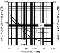
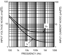
| en | Input Referred Voltage Noise | f ≥ 0.1 MHz | 4.5 | nV/√Hz | ||
| in | Input-Referred Current Noise | f ≥ 0.1 MHz | 1.7 | pA/√Hz | ||
| Second Harmonic Distortion | AV = +1, f = 5 MHz | −80 | dBc | |||
| Third Harmonic Distortion | VO = 2 VPP, RL = 100Ω | −85 | ||||
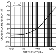
| Xt | Crosstalk (for LMH6655 only) | Input Referred, 5 MHz, Channel-to-Channel | −80 | dB | ||
| DG | Differential Gain | AV = +2, NTSC, RL = 150Ω | 0.01% | |||
| DP | Differential Phase | AV = +2, NTSC, RL = 150Ω | 0.025 | deg | ||
| INPUT CHARACTERISTICS | ||||||
| VOS | Input Offset Voltage | VCM = 0V | −3 −4 |
±1 | 3 4 |
mV |
| TC VOS | Input Offset Average Drift | VCM = 0V (7) | 6 | µV/°C | ||
| IB | Input Bias Current | VCM = 0V | 5 | 12 18 |
µA | |
| IOS | Input Offset Current | VCM = 0V | −1 −2 |
0.3 | 1 2 |
µA |
| RIN | Input Resistance | Common Mode | 4 | MΩ | ||
| Differential Mode | 20 | kΩ | ||||
| CIN | Input Capacitance | Common Mode | 1.8 | pF | ||
| Differential Mode | 1 | |||||
| CMRR | Common Mode Rejection Ration | Input Referred, VCM = 0V to −5V |
70 68 |
90 | dB | |
| CMVR | Input Common- Mode Voltage Range | CMRR ≥ 50 dB | −5.15 | −5.0 | V | |
| 3.5 | 3.7 | |||||
| TRANSFER CHARACTERISTICS | ||||||
| AVOL | Large Signal Voltage Gain | VO = 4 VPP, RL = 100Ω | 60 58 |
67 | dB | |
| OUTPUT CHARACTERISTICS | ||||||
| VO | Output Swing High | No Load | 3.4 3.2 |
3.6 | V | |
| Output Swing Low | No Load | −3.9 | −3.7 −3.5 |
|||
| Output Swing High | RL = 100Ω | 3.2 3.0 |
3.4 | |||
| Output Swing Low | RL = 100Ω | −3.6 | −3.4 −3.2 |
|||
| ISC | Short Circuit Current (3) | Sourcing, VO = 0V ΔVIN = 200 mV |
145 130 |
280 | mA | |
| Sinking, VO = 0V ΔVIN = 200 mV |
100 80 |
185 | ||||
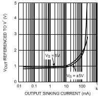
| IOUT | Output Current | Sourcing, VO = +3V | 80 | mA | ||
| Sinking, VO = −3V | 120 | |||||
| RO | Output Resistance | AV = +1, f <100 kHz | 0.08 | Ω | ||
| POWER SUPPLY | ||||||
| PSRR | Power Supply Rejection Ratio | Input Referred, VS = ±5V to ±6V |
60 | 76 | dB | |
| IS | Supply Current (per channel) | 4.5 | 6 7 |
mA | ||
5V Electrical Characteristics
Unless otherwise specified, all limits ensured for V+ = +5V, V− = −0V, VCM = 2.5V, AV = +1, RF = 25 Ω for gain = +1,RF = 402Ω for gain ≥ +2, and RL = 100Ω to V+/2. Boldface limits apply at the temperature extremes.
| PARAMETER | TEST CONDITIONS | MIN(6) | TYP(5) | MAX(6) | UNIT | |
|---|---|---|---|---|---|---|
| DYNAMIC PERFORMANCE | ||||||
| fCL | Close Loop Bandwidth | AV = +1 | 230 | MHz | ||
| AV = +2 | 120 | |||||
| AV = +5 | 50 | |||||
| AV = +10 | 25 | |||||
| GBWP | Gain Bandwidth Product | AV ≥ +5 | 250 | MHz | ||
| Bandwidth for 0.1 dB Flatness | AV = +1 | 17 | MHz | |||
| φm | Phase Margin | 48 | deg | |||
| SR | Slew Rate (8) | AV = +1, VIN = 2 VPP | 190 | V/µs | ||
| tS | Settling Time 0.01% |
AV = +1, 2V Step | 30 | ns | ||
| 0.1% | 20 | ns | ||||
| tr | Rise Time | AV = +1, 0.2V Step | 1.5 | ns | ||
| tf | Fall Time | AV = +1, 0.2V Step | 1.35 | ns | ||
| DISTORTION and NOISE RESPONSE | ||||||
| en | Input Referred Voltage Noise | f ≥ 0.1 MHz | 4.5 | nV/√Hz | ||
| in | Input Referred Current Noise | f ≥ 0.1 MHz | 1.7 | pA/√Hz | ||
| Second Harmonic Distortion | AV = +1, f = 5 MHz | −65 | dBc | |||
| Third Harmonic Distortion | VO = 2 VPP, RL = 100Ω | −70 | ||||
| Xt | Crosstalk (for LMH6655 only) | Input Referred, 5 MHz | −78 | dB | ||
| INPUT CHARACTERISTICS | ||||||
| VOS | Input Offset Voltage | VCM = 2.5V | −5 −6.5 |
±2 | 5 6.5 |
mV |
| TC VOS | Input Offset Average Drift | VCM = 2.5V (7) | 6 | µV/°C | ||
| IB | Input Bias Current | VCM = 2.5V | 6 | 12 18 |
µA | |
| IOS | Input Offset Current | VCM = 2.5V | −2 −3 |
0.5 | 2 3 |
µA |
| RIN | Input Resistance | Common Mode | 4 | MΩ | ||
| Differential Mode | 20 | kΩ | ||||
| CIN | Input Capacitance | Common Mode | 1.8 | pF | ||
| Differential Mode | 1 | |||||
| CMRR | Common Mode Rejection Ration | Input Referred, VCM = 0V to −2.5V |
70 68 |
90 | dB | |
| CMVR | Input Common Mode Voltage Range | CMRR ≥ 50 dB | −0.15 | 0 | V | |
| 3.5 | 3.7 | |||||
| TRANSFER CHARACTERISTICS | ||||||
| AVOL | Large Signal Voltage Gain | VO = 1.6 VPP, RL = 100Ω | 58 55 |
64 | dB | |
| OUTPUT CHARACTERISTICS | ||||||
| VO | Output Swing High | No Load | 3.6 3.4 |
3.75 | V | |
| Output Swing Low | No Load | 0.9 | 1.1 1.3 |
|||
| Output Swing High | RL = 100Ω | 3.5 3.35 |
3.70 | |||
| Output Swing Low | RL = 100Ω | 1 | 1.3 1.45 |
|||
| ISC | Short Circuit Current (3) | Sourcing , VO = 2.5V ΔVIN = 200 mV |
90 80 |
170 | mA | |
| Sinking, VO = 2.5V ΔVIN = 200 mV |
70 60 |
140 | ||||
| IOUT | Output Current | Sourcing, VO = +3.5V | 30 | mA | ||
| Sinking, VO = 1.5V | 60 | |||||
| RO | Output Resistance | AV = +1, f <100 kHz | .08 | Ω | ||
| POWER SUPPLY | ||||||
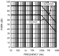
| PSRR | Power Supply Rejection Ratio | Input Referred , VS = ± 2.5V to ± 3V |
60 | 75 | dB | |
| IS | Supply Current (per channel) | 4.5 | 6 7 |
mA | ||
(1) Absolute Maximum Ratings indicate limits beyond which damage to the device may occur. Operating Ratings indicate conditions for which the device is intended to be functional, but specific performance is not ensured. For ensured specifications and the test conditions, see the Electrical Characteristics Table.
(2) Human body model, 1.5 kΩ in series with 100 pF. Machine model: 0Ω in series with 100 pF.
(3) Continuous short circuit operation at elevated ambient temperature can result in exceeding the maximum allowed junction temperature at 150°C.
(4) The maximum power dissipation is a function of TJ(MAX), RθJA and TA. The maximum allowable power dissipation at any ambient temperature is PD = (TJ(MAX) − TA)/RθJA. All numbers apply for packages soldered directly onto a PC board.
(5) Typical Values represent the most likely parametric norm.
(6) All limits are specified by testing or statistical analysis.
(7) Offset voltage average drift is determined by dividing the change in VOS at temperature extremes into the total temperature change.
(8) Slew rate is the slower of the rising and falling slew rates. Slew rate is rate of change from 10% to 90% of output voltage step.
6.5 Typical Characteristics
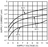
25°C, V+ = ±5 V, V− = −5, RF = 25 Ω for gain = +1, RF = 402 Ω for gain ≥ +2 and RL = 100 Ω, unless otherwise specified.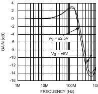
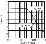
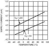
vs. Supply Voltage
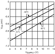 Figure 7. Offset Voltage
vs. Supply Voltage (VCM = 0V)
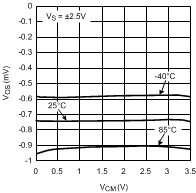 Figure 9. Offset Voltage
vs. Common Mode
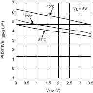 Figure 11. Bias Current
vs. Common Mode Voltage
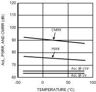 Figure 13. AOL, PSRR and CMRR
vs. Temperature
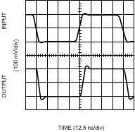
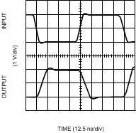 Figure 15. Inverting Large Signal Pulse Response
(VS = ±5V)
 Figure 17. Non-Inverting Large Signal Pulse Response
 (VS = ±5V)
(VS = ±5V)

(VS = ±5V)
vs. Frequency (VS = ±5V)
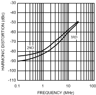
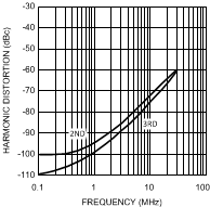 Figure 25. Harmonic Distortion
vs. Frequency
G = +1, VO = 2 VPP, VS = ±5V
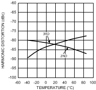 Figure 27. Harmonic Distortion
vs. Temperature
VS = ±5V, f = 5 MHz, VO = 2 VPP
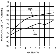 Figure 29. Harmonic Distortion
vs. Gain
VS = ±5V, f = 5 MHz, VO = 2 VPP
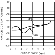
vs. Output Swing
(G = +2, VS = ±5V, f = 5 MHz)
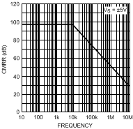
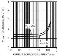
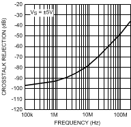 Figure 37. CrossTalk
vs. Frequency (LMH6655 only)
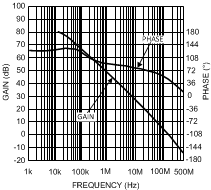 Figure 39. Open Loop Gain and Phase
vs. Frequency
vs. Temperature
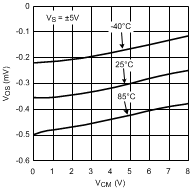 Figure 8. Offset Voltage
vs. Common Mode
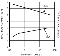 Figure 10. Bias Current and Offset Voltage
vs. Temperature
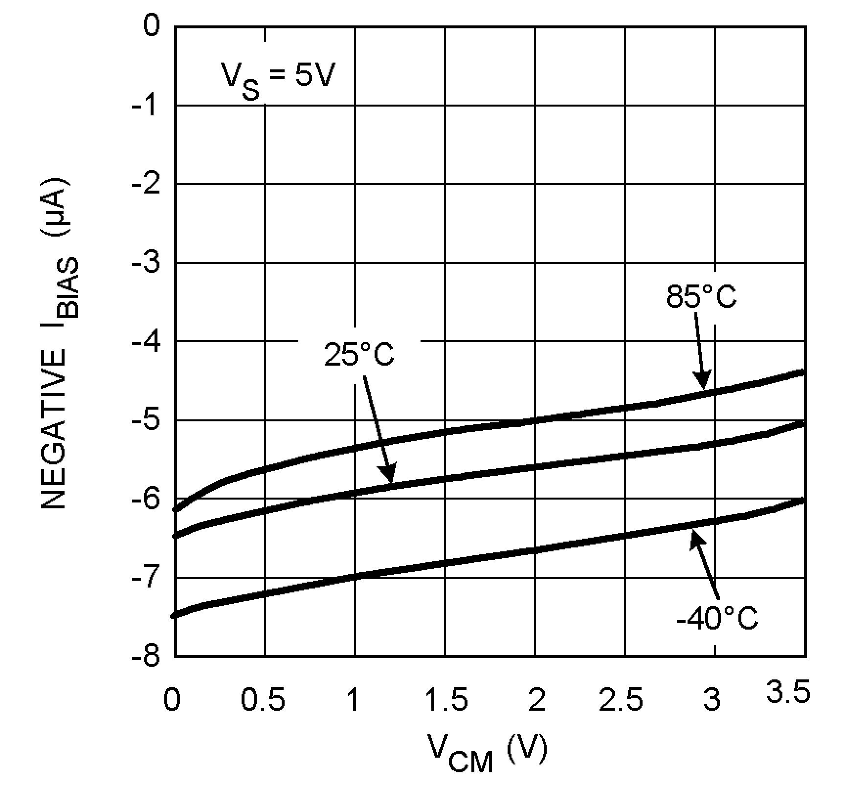 Figure 12. Bias Current
vs. Common Mode Voltage
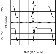
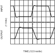 Figure 14. Inverting Large Signal Pulse Response
 (VS = 5V)
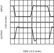
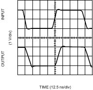 Figure 16. Non-Inverting Large Signal Pulse Response
 (VS = 5V)
(VS = 5V)
(VS = 5V)
vs. Frequency (VS = 5V)
vs. Frequency
G = +1, VO = 2 VPP, VS = 5V
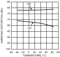 Figure 26. Harmonic Distortion
vs. Temperature
VS = 5V, f = 5 MHz, VO = 2 VPP
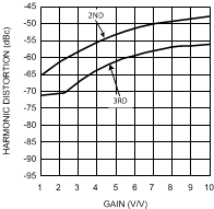 Figure 28. Harmonic Distortion
vs. Gain
VS = 5V, f = 5 MHz, VO = 2 VPP
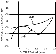 Figure 30. Harmonic Distortion
vs. Output Swing
(G = +2, VS = 5V, f = 5 MHz)
vs. Frequency (LMH6655 only)
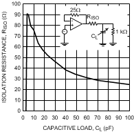 Figure 38. Isolation Resistance
vs. Capacitive Load