SNVS174I February 2003 – February 2015 LP3852 , LP3855
PRODUCTION DATA.
- 1 Features
- 2 Applications
- 3 Description
- 4 Simplified Schematics
- 5 Revision History
- 6 Voltage Options
- 7 Pin Configuration and Functions
- 8 Specifications
- 9 Detailed Description
-
10Application and Implementation
- 10.1 Application Information
- 10.2
Typical Applications
- 10.2.1 Design Requirements
- 10.2.2 Detailed Design Procedure
- 10.2.3 Application Curves
- 11Power Supply Recommendations
- 12Layout
- 13Device and Documentation Support
- 14Mechanical, Packaging, and Orderable Information
Package Options
Mechanical Data (Package|Pins)
Thermal pad, mechanical data (Package|Pins)
Orderable Information
12 Layout
12.1 Layout Guidelines
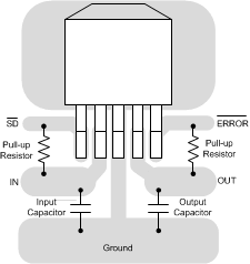
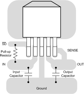
Good PC layout practices must be used or instability can be induced because of ground loops and voltage drops. The input and output capacitors must be directly connected to the IN, OUT, and ground pins of the regulator using traces which do not have other currents flowing in them (Kelvin connect).
The best way to do this is to lay out CIN and COUT near the device with short traces to the IN, OUT, and ground pins. The regulator ground pin should be connected to the external circuit ground so that the regulator and its capacitors have a "single point ground".
It should be noted that stability problems have been seen in applications where "vias" to an internal ground plane were used at the ground points of the IC and the input and output capacitors. This was caused by varying ground potentials at these nodes resulting from current flowing through the ground plane. Using a single point ground technique for the regulator and its capacitors fixed the problem.
Since high current flows through the traces going into IN and coming from OUT, Kelvin connect the capacitor leads to these pins so there is no voltage drop in series with the input and output capacitors.
12.2 Layout Example
 Figure 24. LP3852 TO-263 Package Typical Layout
 Figure 25. LP3855 TO-263 Package Typical Layout
12.3 RFI and/or EMI Susceptibility
Radio frequency interference (RFI) and electromagnetic interference (EMI) can degrade any integrated circuit performance because of the small dimensions of the geometries inside the device. In applications where circuit sources are present which generate signals with significant high frequency energy content (> 1 MHz), care must be taken to ensure that this does not affect the device regulator.
If RFI and/or EMI noise is present on the input side of the regulator (such as applications where the input source comes from the output of a switching regulator), good ceramic bypass capacitors must be used at the IN pin of the device.
If a load is connected to the device output which switches at high speed (such as a clock), the high-frequency current pulses required by the load must be supplied by the capacitors on the device output. Since the bandwidth of the regulator loop is less than 100 kHz, the control circuitry cannot respond to load changes above that frequency. This means the effective output impedance of the device at frequencies above 100 kHz is determined only by the output capacitor or capacitors.
In applications where the load is switching at high speed, the output of the IC may need RF isolation from the load. It is recommended that some inductance be placed between the output capacitor and the load, and good RF bypass capacitors be placed directly across the load.
PCB layout is also critical in high noise environments, since RFI and/or EMI is easily radiated directly into PC traces. Noisy circuitry should be isolated from "clean" circuits where possible, and grounded through a separate path. At MHz frequencies, ground planes begin to look inductive and RFI and/or EMI can cause ground bounce across the ground plane.
In multi-layer PCB applications, care should be taken in layout so that noisy power and ground planes do not radiate directly into adjacent layers which carry analog power and ground.
12.4 Power Dissipation/Heatsinking
The LP3852 and LP3855 can deliver a continuous current of 1.5 A over the full operating temperature range. A heatsink may be required depending on the maximum power dissipation and maximum ambient temperature of the application. Under all possible conditions, the junction temperature must be within the range specified under operating conditions. The total power dissipation of the device is given by:
where
- IGND is the operating ground current of the device (specified under Electrical Characteristics).
The maximum allowable temperature rise (TRmax) depends on the maximum ambient temperature (TAmax) of the application, and the maximum allowable junction temperature (TJmax):
The maximum allowable value for junction to ambient thermal resistance, RθJA, can be calculated using the formula:
The LP3852 and LP3855 are available in TO-220 and TO-263 packages. The thermal resistance depends on amount of copper area or heat sink, and on air flow. If the maximum allowable value of RθJA calculated in Equation 3 is ≥ 60 °C/W for TO-220 package and ≥ 60°C/W for TO-263 package, no heatsink is needed since the package can dissipate enough heat to satisfy these requirements. If the value for allowable RθJA falls below these limits, a heat sink is required.
12.4.1 Heatsinking TO-220 Package
The thermal resistance of a TO-220 package can be reduced by attaching it to a heat sink or a copper plane on a PC board. If a copper plane is to be used, the values of RθJA will be same as shown in next section for TO-263 package.
The heatsink to be used in the application should have a heatsink to ambient thermal resistance,
RθHA≤ RθJA − RθCH − RθJC.
In this equation, RθCH is the thermal resistance from the case to the surface of the heat sink, and RθJC is the thermal resistance from the junction to the surface of the case. RθJC is about 3°C/W for a TO-220 package. The value for RθCH depends on method of attachment, insulator, etc. RθCH varies between 1.5°C/W to 2.5°C/W. If the exact value is unknown, 2°C/W can be assumed.
12.4.2 Heatsinking TO-263 Package
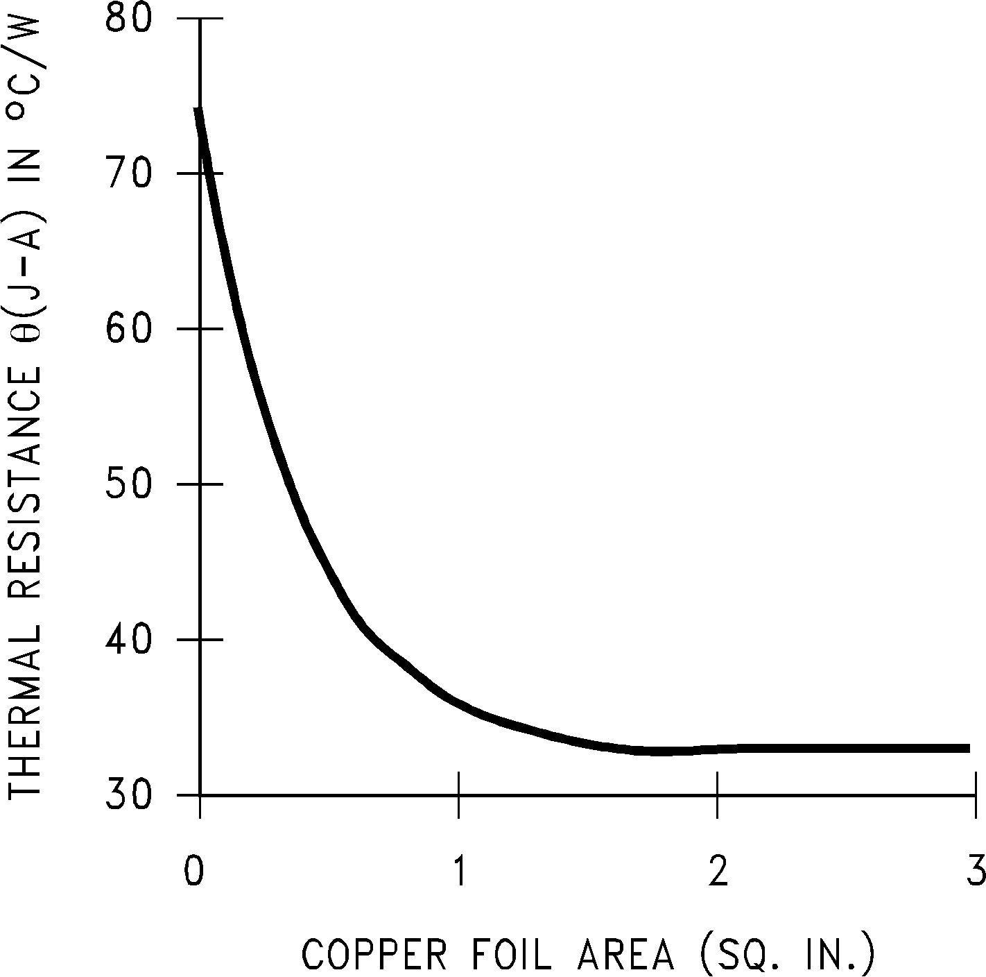
The TO-263 package uses the copper plane on the PCB as a heatsink. The tab of these packages are soldered to the copper plane for heat sinking. Figure 26 shows a curve for the RθJA of TO-263 package for different copper area sizes, using a typical PCB with 1 ounce copper and no solder mask over the copper area for heat sinking.
 Figure 26. RθJA vs Copper (1 Ounce) Area for TO-263 package
As shown in the figure, increasing the copper area beyond 1 square inch produces very little improvement. The minimum value for RθJA for the TO-263 package mounted to a PCB is 32°C/W.
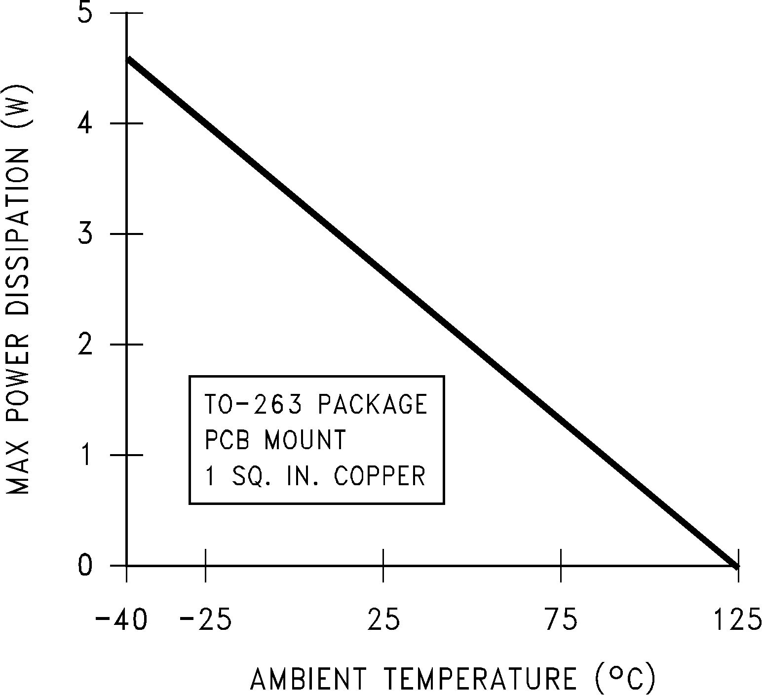
Figure 27 shows the maximum allowable power dissipation for TO-263 packages for different ambient temperatures, assuming RθJA is 35°C/W and the maximum junction temperature is 125°C.
