SLLS236I October 1996 – June 2015 SN65LBC184 , SN75LBC184
PRODUCTION DATA.
- 1 Features
- 2 Applications
- 3 Description
- 4 Revision History
- 5 Pin Configuration and Functions
-
6 Specifications
- 6.1 Absolute Maximum Ratings
- 6.2 ESD Ratings
- 6.3 Recommended Operating Conditions
- 6.4 Thermal Information
- 6.5 Electrical Characteristics: Driver
- 6.6 Electrical Characteristics: Receiver
- 6.7 Driver Switching Characteristics
- 6.8 Receiver Switching Characteristics
- 6.9 Dissipation Ratings
- 6.10 Typical Characteristics
- 7 Parameter Measurement Information
- 8 Detailed Description
- 9 Application and Implementation
- 10Power Supply Recommendations
- 11Layout
- 12Device and Documentation Support
- 13Mechanical, Packaging, and Orderable Information
Package Options
Mechanical Data (Package|Pins)
Thermal pad, mechanical data (Package|Pins)
Orderable Information
8 Detailed Description
8.1 Overview
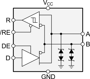
The SNx5LBC184 device is a 5-V, half-duplex, RS-485 transceiver with integrated transient voltage suppressors that prevent circuit damage in the presence of high-energy transients of up to 400-W peak power. This transceiver has an active-HIGH driver enable and active-LOW receiver enable. The differential driver is suitable for data transmission up to 250 kbps.
8.2 Functional Block Diagram
 Figure 13. Functional Logic Diagram
8.3 Feature Description
Integrated transient voltage suppressors protect the transceiver against Electrostatic Discharges (ESD) according to IEC 61000-4-2 of up to ±30 kV and surge transients according to IEC 61000-4-5 of up to 400-W peak.
The differential driver incorporates slew-rate controlled outputs sufficient to transmit data up to 250 kbps. Slew-rate control allows for longer unterminated cable runs and longer stub lengths from the main cable trunk than with faster voltage transitions. A unique receiver design provides a high level failsafe output when the inputs are left floating.
The SN65LBC184 is characterized from –40°C to 85°C and the SN75LBC184 is characterized from 0°C to 70°C.
8.4 Device Functional Modes
When the driver enable pin (DE) is logic high, the differential outputs A and B follow the logic states at data input D. A logic high at D causes A to turn high and B to turn low. In this case, the differential output voltage defined as VOD = VA – VB is positive. When D is low, the output states reverse, B turns high, A becomes low, and VOD is negative.
When DE is low, both outputs turn high-impedance. In this condition, the logic state at D is irrelevant.
Table 1. Driver Functions(1)
| INPUT | ENABLE | OUTPUTS | FUNCTION | |
|---|---|---|---|---|
| D | DE | A | B | |
| H | H | H | L | Actively drive bus High |
| L | H | L | H | Actively drive bus Low |
| X | L | Z | Z | Driver disabled |
Z = high impedance (off)
When the receiver enable pin, RE, is logic low, the receiver is enabled. When the differential input voltage defined as VID = VA – VB is positive and higher than the positive input threshold, VIT+, the receiver output (R) turns high. When VID is negative and lower than the negative input threshold, VIT–, the receiver output turns low. If VID is between VIT+ and VIT–, the output is indeterminate.
When RE is logic high, the receiver output is high-impedance and the magnitude and polarity of VID are irrelevant. When the transceiver is disconnected from the bus, the receiver provides a failsafe high output.
Table 2. Receiver Functions(1)
| DIFFERENTIAL INPUT | ENABLE | OUTPUT | FUNCTION |
|---|---|---|---|
| VID = VA – VB | RE | R | |
| VID > VIT+ | L | H | Receive valid bus High |
| VIT– < VID < VIT+ | L | ? | Indeterminate bus state |
| VID < VIT– | L | L | Receive valid bus Low |
| X | H | Z | Receiver disabled |
| OPEN | L | H | Receiver failsafe High |
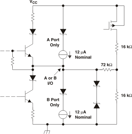
 Figure 14. Schematic of Inputs and Outputs