SLLS236I October 1996 – June 2015 SN65LBC184 , SN75LBC184
PRODUCTION DATA.
- 1 Features
- 2 Applications
- 3 Description
- 4 Revision History
- 5 Pin Configuration and Functions
-
6 Specifications
- 6.1 Absolute Maximum Ratings
- 6.2 ESD Ratings
- 6.3 Recommended Operating Conditions
- 6.4 Thermal Information
- 6.5 Electrical Characteristics: Driver
- 6.6 Electrical Characteristics: Receiver
- 6.7 Driver Switching Characteristics
- 6.8 Receiver Switching Characteristics
- 6.9 Dissipation Ratings
- 6.10 Typical Characteristics
- 7 Parameter Measurement Information
- 8 Detailed Description
- 9 Application and Implementation
- 10Power Supply Recommendations
- 11Layout
- 12Device and Documentation Support
- 13Mechanical, Packaging, and Orderable Information
Package Options
Mechanical Data (Package|Pins)
Thermal pad, mechanical data (Package|Pins)
Orderable Information
6 Specifications
6.1 Absolute Maximum Ratings
over operating free-air temperature range (unless otherwise noted) (1)| MIN | MAX | UNIT | ||||
|---|---|---|---|---|---|---|
| VCC | Supply voltage(2) | –0.5 | 7 | V | ||
| Continuous voltage range at any bus terminal | –15 | 15 | V | |||
| Data input/output voltage | –0.3 | 7 | V | |||
| IO | Receiver output current | –20 | 20 | mA | ||
| Continuous total power dissipation(3) | Internally Limited | |||||
| Tstg | Storage temperature | 160 | °C | |||
(1) Stresses beyond those listed under Absolute Maximum Ratings may cause permanent damage to the device. These are stress ratings only, and functional operation of the device at these or any other conditions beyond those indicated under Recommended Operating Conditions is not implied. Exposure to absolute-maximum-rated conditions for extended periods may affect device reliability.
(2) All voltage values, except differential input/output bus voltage, are with respect to network ground terminal.
(3) The driver shuts down at a junction temperature of approximately 160°C. To operate below this temperature, see the Dissipation Ratings.
6.2 ESD Ratings
| VALUE | UNIT | ||||
|---|---|---|---|---|---|
| V(ESD) | Electrostatic discharge | Human body model (HBM), per ANSI/ESDA/JEDEC JS-001(1) | A, B, GND | ±15000 | V |
| All pins | ±3000 | ||||
| Contact discharge (IEC61000-4-2) | A, B, GND(2) | ±30000 | |||
| Air discharge (IEC61000-4-2) | A, B, GND(3) | ±15000 | |||
| All pins (Class 3A) | ±8000 | ||||
| All pins (Class 3B) | ±200 | ||||
(1) JEDEC document JEP155 states that 500-V HBM allows safe manufacturing with a standard ESD control process.
(2) GND and bus pin ESD protection is beyond readily available test equipment capabilities for IEC 61000-4-2, EIA/JEDEC test method A114-A and MIL-STD-883C method 3015. Ratings listed are limits of test equipment; device performance exceeds these limits.
6.3 Recommended Operating Conditions
over operating free-air temperature range (unless otherwise noted)| MIN(1) | TYP | MAX | UNIT | |||
|---|---|---|---|---|---|---|
| VCC | Supply voltage | 4.75 | 5 | 5.25 | V | |
| VI or VIC | Voltage at any bus terminal (separately or common mode) | –7 | 12 | V | ||
| VIH | High-level input voltage | D, DE, and RE | 2 | V | ||
| VIL | Low-level input voltage | D, DE, and RE | 0.8 | V | ||
| |VID| | Differential input voltage | 12 | V | |||
| IOH | High-level output current | Driver | –60 | mA | ||
| Receiver | –8 | |||||
| IOL | Low-level output current | Driver | 60 | mA | ||
| Receiver | 4 | |||||
| TA | Operating free-air temperature | SN75LBC184 | 0 | 70 | °C | |
| SN65LBC184 | –40 | 85 | ||||
(1) The algebraic convention, in which the less-positive (more-negative) limit is designated minimum, is used in this data sheet.
6.4 Thermal Information
| THERMAL METRIC(1) | SNx5LBC184 | UNIT | ||
|---|---|---|---|---|
| P [PDIP] | D [SOIC] | |||
| 8 PINS | ||||
| RθJA | Junction-to-ambient thermal resistance | 108.7 | 172.4 | °C/W |
| RθJC(top) | Junction-to-case (top) thermal resistance | 34.8 | 42.5 | °C/W |
| RθJB | Junction-to-board thermal resistance | 23.6 | 41.4 | °C/W |
| ψJT | Junction-to-top characterization parameter | 12 | 4.6 | °C/W |
| ψJB | Junction-to-board characterization parameter | 23.5 | 40.7 | °C/W |
| RθJC(bot) | Junction-to-case (bottom) thermal resistance | N/A | N/A | °C/W |
(1) For more information about traditional and new thermal metrics, see the Semiconductor and IC Package Thermal Metrics application report, SPRA953.
6.5 Electrical Characteristics: Driver
over recommended operating conditions (unless otherwise noted)| PARAMETER | ALTERNATE SYMBOLS | TEST CONDITIONS | MIN | TYP(1) | MAX | UNIT | ||
|---|---|---|---|---|---|---|---|---|
| ICC | Supply current | NA | DE = RE = 5 V | No Load | 12 | 25 | mA | |
| DE = 0 V RE = 5 V |
No Load |
175 | 300 | μA | ||||
| IIH | High-level input current (D, DE, RE) | NA | VI = 2.4 V | 50 | μA | |||
| IIL | Low-level input current (D, DE, RE) | NA | VI = 0.4 V | –50 | μA | |||
| IOS | Short-circuit output current OS(2) | NA | VO = –7 V | –250 | –120 | mA | ||
| VO = VCC | 250 | |||||||
| VO = 12 V | 250 | |||||||
| IOZ | High-impedance output current | NA | See Receiver II | mA | ||||
| VO | Output voltage | Voa, Vob | IO = 0 | 0 | VCC | V | ||
| VOC(PP) | Peak-to-peak change in common-mode output voltage during state transitions | NA | See Figure 9 and Figure 10 | 0.8 | V | |||
| VOC | Common-mode output voltage | |Vos| | See Figure 8 | 1 | 3 | V | ||
| |ΔVOC(SS)| | Magnitude of change, common-mode steady-state output voltage | |Vos – Vos| | See Figure 10 | 0.1 | V | |||
| |VOD| | Magnitude of differential output voltage |VA – VB| | Vo | IO = 0 | 1.5 | 6 | V | ||
| RL = 54 Ω, See Figure 8 | 1.5 | V | ||||||
| Δ|VOD| | Change in differential voltage magnitude between logic states | ||Vt| – |Vt|| | RL = 54 Ω | 0.1 | V | |||
(1) All typical values are measured with TA = 25°C and VCC = 5 V.
(2) This parameter is measured with only one output being driven at a time.
6.6 Electrical Characteristics: Receiver
over recommended operation conditions (unless otherwise noted)| PARAMETER | TEST CONDITIONS | MIN | TYP(1) | MAX | UNIT | ||
|---|---|---|---|---|---|---|---|
| ICC | Supply current (total package) | DE = RE = 0 V, No Load | 3.9 | mA | |||
| RE = 5 V, DE = 0 V, No Load | 300 | μA | |||||
| II | Input current | Other input = 0 V | VI = 12 V | 250 | μA | ||
| VI = 12 V, VCC = 0 | 250 | ||||||
| VI = –7 V | –200 | ||||||
| VI = –7 V, VCC = 0 | –200 | ||||||
| IOZ | High-impedance-state output current | VO = 0.4 V to 2.4 V | ±100 | μA | |||
| Vhys | Input hysteresis voltage | 70 | mV | ||||
| VIT+ | Positive-going input threshold voltage | 200 | V | ||||
| VIT– | Negative-going input threshold voltage | –200 | mV | ||||
| VOH | High-level output voltage | IOH = –8 mA, See Figure 11 | 2.8 | V | |||
| VOL | Low-level output voltage | IOL = 4 mA, See Figure 11 | 0.4 | V | |||
(1) All typical values are at VCC = 5 V, TA = 25°C.
6.7 Driver Switching Characteristics
over recommended operating conditions (unless otherwise noted)| PARAMETER | TEST CONDITIONS | MIN | TYP | MAX | UNIT | ||
|---|---|---|---|---|---|---|---|
| td(DH) | Differential output delay time, low-to-high-level output | RL = 54 Ω CL = 50 pF |
See Figure 9 | 1.3 | μs | ||
| td(DL) | Differential output delay time, high-to-low-level output | 1.3 | μs | ||||
| tPLH | Propagation delay time, low-to-high-level output | 0.5 | 1.3 | μs | |||
| tPHL | Propagation delay time, high-to-low-level output | 0.5 | 1.3 | μs | |||
| tsk(p) | Pulse skew (| td(DH) – td(DL)|) | 75 | 150 | ns | |||
| tr | Rise time, single-ended | 0.25 | 1.2 | μs | |||
| tf | Fall time, single-ended | 0.25 | 1.2 | μs | |||
| tPZH | Output enable time to high level | RL = 110 Ω | See Figure 6 | 3.5 | μs | ||
| tPZL | Output enable time to low level | RL = 110 Ω | See Figure 7 | 3.5 | μs | ||
| tPHZ | Output disable time from high level | RL = 110 Ω | See Figure 6 | 2 | μs | ||
| tPLZ | Output disable time from low level | RL = 110 Ω | See Figure 7 | 2 | μs | ||
6.8 Receiver Switching Characteristics
over recommended operating conditions (unless otherwise noted)| PARAMETER | TEST CONDITIONS | MIN | TYP | MAX | UNIT | ||
|---|---|---|---|---|---|---|---|
| tPLH | Propagation delay time, low-to-high-level output | CL = 50 pF, See Figure 11 | 150 | ns | |||
| tPHL | Propagation delay time, high-to-low-level output | 150 | ns | ||||
| tsk(p) | Pulse skew (|tPHL– tPLH|) | 50 | ns | ||||
| tr | Rise time, single-ended | See Figure 11 | 20 | ns | |||
| tf | Fall time, single-ended | 20 | ns | ||||
| tPZH | Output enable time to high level | See Figure 12 | 100 | ns | |||
| tPZL | Output enable time to low level | 100 | ns | ||||
| tPHZ | Output disable time from high level | 100 | ns | ||||
| tPLZ | Output disable time from low level | 100 | ns | ||||
6.9 Dissipation Ratings
| PACKAGE | TA ≤ 25°C POWER RATING |
DERATING FACTOR ABOVE TA = 25°C |
TA = 70°C POWER RATING |
TA = 85°C POWER RATING |
|---|---|---|---|---|
| D | 725 mW | 5.8 mW/°C | 464 mW | 377 mW |
| P | 1150 mW | 9.2 mW/°C | 736 mW | 598 mW |
6.10 Typical Characteristics
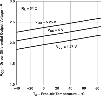 Figure 1. Driver Differential Output Voltage vs Free-Air Temperature
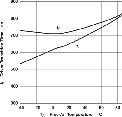 Figure 3. Driver Transition Time vs Free-Air Temperature
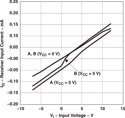 Figure 5. Receiver Input Current vs Input Voltage
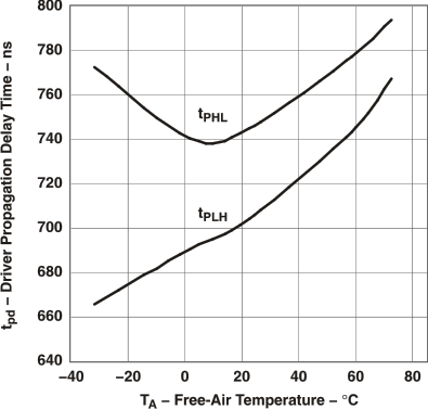 Figure 2. Driver Propagation Delay Time vs Free-Air Temperature
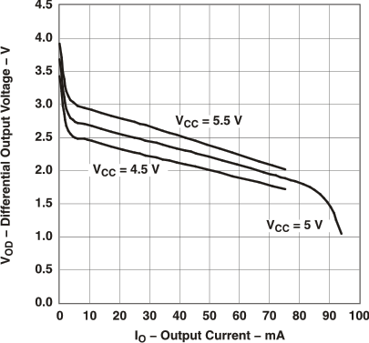 Figure 4. Differential Output Voltage vs Output Current