SBOS780C March 2016 – June 2021 THS3215
PRODUCTION DATA
- 1 Features
- 2 Applications
- 3 Description
- 4 Revision History
- 5 Pin Configuration and Functions
-
6 Specifications
- 6.1 Absolute Maximum Ratings
- 6.2 ESD Ratings
- 6.3 Recommended Operating Conditions
- 6.4 Thermal Information
- 6.5 Electrical Characteristics: D2S
- 6.6 Electrical Characteristics: OPS
- 6.7 Electrical Characteristics: D2S + OPS
- 6.8 Electrical Characteristics: Midscale (DC) Reference Buffer
- 6.9 Typical Characteristics: D2S + OPS
- 6.10 Typical Characteristics: D2S Only
- 6.11 Typical Characteristics: OPS Only
- 6.12 Typical Characteristics: Midscale (DC) Reference Buffer
- 6.13 Typical Characteristics: Switching Performance
- 6.14 Typical Characteristics: Gain Drift
- 7 Parameter Measurement Information
-
8 Detailed Description
- 8.1 Overview
- 8.2 Functional Block Diagram
- 8.3 Feature Description
- 8.4 Device Functional Modes
-
9 Application and Implementation
- 9.1
Application Information
- 9.1.1
Typical Applications
- 9.1.1.1 High-Frequency, High-Voltage, Dual-Output Line Driver for AWGs
- 9.1.1.2 High-Voltage Pulse-Generator
- 9.1.1.3 Single-Supply, AC-Coupled, Piezo Element Driver
- 9.1.1.4 Output Common-Mode Control Using the Midscale Buffer as a Level Shifter
- 9.1.1.5 Differential I/O Driver With independent Common-Mode Control
- 9.1.1
Typical Applications
- 9.1
Application Information
- 10Power Supply Recommendations
- 11Layout
- 12Device and Documentation Support
- 13Mechanical, Packaging, and Orderable Information
Package Options
Mechanical Data (Package|Pins)
- RGV|16
Thermal pad, mechanical data (Package|Pins)
Orderable Information
8.3.1 Differential to Single-Ended Stage (D2S) With Fixed Gain of 2 V/V (Pins 2, 3, 6, and 14)
This buffered-amplifier stage isolates the DAC output pins from the differential to single-ended conversion. Present two high-impedance inputs to allow the DAC to operate in its best configuration independent of subsequent operations. The two very wideband input buffers hold an approximately constant response shape over a wide input common-mode operating voltage. Figure 6-13 shows 6 dB of gain with 0.5 dB flatness through 100 MHz over the intended –1 V to +3 V input common-mode range. In this case, the VREF pin is grounded, forcing the D2S output to be centered on ground for any input common-mode voltage. For the D2S-only tests, a 100 Ω load is used to showcase the performance of this stage directly driving a doubly-terminated cable. The wide, input common-mode range of the D2S satisfies the required compliance voltage over a wide range of DAC types. Most current sourcing DACs require an average dc compliance voltage on their outputs near ground. Current sinking DACs require an average dc compliance voltage near their positive supply voltage for the analog section. The 3 V maximum common-mode range is intended to support DAC supplies up to 3.3 V, where the average output operating current pulls down from 3.3 V by the termination impedance from the supply. For instance, a 20 mA tail current DAC must level shift from a 3.3 V bias on the output resistors down to 3 V or lower. This DAC-to-THS3215 configuration requires at least a 300 mV dc level shift with half the tail current in each side, implying a 30 Ω load impedance to the supply on each output side using a 20 mA reference current.
The overriding limits to the input common-mode operating range are due to the input buffer headroom. Over temperature, the D2S input headroom specification is 2 V to the negative supply and 1.5 V to the positive supply. Therefore, operation at a 3 V input common-mode voltage requires at least a 4.5 V positive supply, where 5 V is a more conservative minimum.
While DAC outputs rarely have any common-mode signal present (unless the reference current is being modulated), the D2S does a reasonable job of rejecting input common-mode signals over frequency. Figure 6-17 shows the CMRR to decrease above 10 MHz. For current-sinking DACs coming from a positive supply voltage, any noise on the positive supply looks like an input common-mode signal. Keeping the noise low at higher frequencies reduces the possibility of feedthrough to the D2S output due to the decreasing CMRR at higher frequencies. A current-sinking DAC uses pull-up resistors to the voltage supply to convert the DAC output current to a voltage. Make sure that the DAC voltage supply is properly decoupled through a ferrite-bead-and-capacitor, π-filter network, similar to the supply decoupling for the THS3215 shown in Figure 8-15.
The D2S provides a differential gain of 6 dB. The gain is reasonably precise using internal resistor matching with extremely low gain drift over temperature (see Figure 6-61 and Figure 6-62). The single-ended D2S output signal can be placed over a wide range of dc offset levels using the VREF pin. The VREF pin shows a precise gain of 1 V/V to the D2S output. Grounding VREF places the first stage output centered on ground (with some offset voltage). For best ac performance through the D2S, anything driving the VREF pin must have a very wide bandwidth with very low output impedance over frequency while driving a 150 Ω load. The on-chip midscale buffer provides these features (see Figure 6-51). When a dc offset (or other small-level ac signal) must be applied to the VREF pin, buffer the signal through the midscale buffer stage. Maintain the total range of the dc offset plus signal swing within the available output swing range of the D2S. The headroom to the supplies is a symmetric ±2.1 V (maximum) over temperature. Therefore, on the minimum ±4 V supply, the D2S operates over a ±1.9 V output range. At the maximum ±7.9 V supply, a ±5.8 V output range is supported. At the higher swings, account for available linear output current, including the current into the internal feedback resistor load of approximately 500-Ω.
Figure 8-1 shows the internal structure of the D2S functional block. It consists of two internal stages:
- The first stage consists of two wideband, closed-loop, fixed gain of 1 V/V buffers to isolate the requirements of the complementary DAC output from the difference operation of the D2S.
- The second stage is a wideband CFA configured as a difference amplifier, operating in a fixed gain of 2 V/V, performing the differential to single-ended conversion.
 Figure 8-1 D2S
Operating Example
Figure 8-1 D2S
Operating ExampleThe CFA design offers the best, full-power bandwidth versus supply current, with moderate noise and dc precision. Figure 8-1 shows a typical current-sourcing DAC with a 20 mA total tail current. The tail current is split equally between the 25 Ω termination resistors to produce a dc common-mode voltage and a differential ac current signal. This example sets the input common-mode voltage at 0.25 V, and is also the compliance voltage of the DAC. The 25 Ω termination resistors shown here are typically realized as a 50 Ω matched reconstruction (or Nyquist) filter between the DAC and the THS3215 buffer inputs for most AWG applications. The DAC signal is further amplified by 6 dB in the second stage for a net transimpedance gain of 100 Ω to the D2S output at VO1. This configuration produces a 2 VPP output for the 20 mA reference current assumed in the example of Figure 8-1. The input common-mode voltage is cancelled on the two sides of the op amp circuit to give a ground referenced output. Any voltage applied to VREF (pin 14) has a gain transfer function of 1 V/V to VO1, independent of the signal path, as long as the source impedance of VREF is very low at dc and over frequency.
The IN+ buffer output drives a 150 Ω load with VREF grounded. Any source driving VREF must have the ability to drive a 150 Ω load with low output impedance across frequency. For differential input signals, the IN– buffer drives a 150 Ω active load. The active load is realized by a combination of the 250 Ω RG resistor and the inverted and attenuated signal present at the inverting terminal of the difference amplifier stage. If only IN– is driven (with IN+ at a dc fixed level), the load is 250 Ω.
The resistor values around the D2S difference amplifier are derived in the following sequence, as shown in Figure 8-2:
- Select the feedback resistor value to set the response shape for the wideband CFA stage. The 500 Ω design used here was chosen as a compromise between loading and noise.
- Set the input resistor on the inverting input side to give the desired single-sided gain for that path. Setting RG= 250 Ω results in a gain of –2 V/V from the buffered signal (–V) to the output of the difference amplifier.
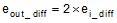
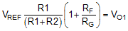
- Solve the required attenuation to the noninverting input to get a matched gain magnitude for the signal provided at the buffer output (+V) on the noninverting path. If α = R2 / (R1 + R2), as shown in Figure 8-2, then the solution for α is shown in Equation 2:
Equation 1.
 Equation 2.
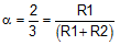
 Figure 8-2 D2S Impedance Analysis
 - After solving the attenuation from the buffer output to the amplifier noninverting input, set the impedance
(R1 + R2). It is preferable to have the two first-stage buffer outputs drive the same load impedance to match nonlinearity in their outputs in order to improve even-order harmonic distortion. The load impedance from –V to RG has an active impedance because of the inverted and attenuated version of the input signal appearing at the inverting amplifier node from the +V input signal. Assuming a positive input signal into the +V path, an attenuated version of the signal appears at the amplifier summing junction side of RG, while the inverted version of the signal appears on the input side of RG.
The impedance seen at node –V in Figure 8-2 is derived in Equation 3 by solving for the V/I expression across RG.
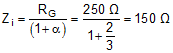
For load balancing, (R1 + R2) = 150 Ω while the attenuation is α. More generally, all the terms are now available to solve for R2, as shown in Equation 4:
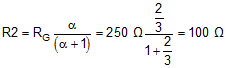
R1 is then simply (Zi – R2) = 50 Ω.
This analysis for matched gains and buffer loads can be applied to a more general, discrete design using different target gains and starting RF values. It is clearly useful to have the attenuation and buffer loading accurately controlled. Therefore, it is very important to control the impedance at VREF (pin 14) to be as low as possible. For instance, using the midscale buffer to drive VREF only adds 0.21 Ω dc impedance in series with R2. This low, dc output impedance can only be delivered with a closed-loop buffer design. For discrete implementations of this D2S, consider the BUF602 buffer and LMH6702 wideband CFA. For even better dc and ac output impedance in the buffers (and possibly better gain), use a closed-loop, dual, wideband op amp like the OPA2889 for lower frequency applications, or the OPA2822 for higher frequency. These unity gain stable op amps can be used as buffers, offering different performance options along with the LMH6702 wideband CFA over the design point chosen for the THS3215.
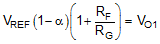
After gain matching is achieved in the single op amp differential stage, the common-mode input voltage is cancelled to the output, and the VREF input voltage is amplified by 1 V/V to the output. The analysis circuit is shown in Figure 8-3, where VREF is shown grounded at the R2 element.
 Figure 8-3 D2S Common-Mode Cancellation
The gain magnitudes are equal on each side of the differential inputs; therefore, the common-mode inputs achieve the same gain magnitude, but opposite phase, resulting in common-mode signal cancellation. The inverting path gain is VCM × (RF / RG). The noninverting path gain is VCM × α × (1 + RF / RG). Using Equation 5:

the noninverting path gain becomes +VCM × RF / RG, and adding that result to the inverting path signal cancels the input common-mode voltage to zero. Slight gain mismatches reduce this rejection to the 48 dB typical CMRR, with a 42 dB tested minimum. The 42 dB minimum over the 3 V maximum common-mode input range adds another ±23.8 mV worst-case D2S output offset term to the specified maximum ±35 mV output offset with 0 V input common-mode voltage. The polarity of the gain mismatch is random.
The VREF pin input voltage (VREF) generates a gain of 1 V/V using the analysis shown in Figure 8-4.
 Figure 8-4 Gain Transfer Function from VREF to VO1
The gain from VREF to VO1 is shown in Equation 6:
Getting both R1 and (R1 + R2) in terms of RG and the target attenuation, α simplifies, as shown in Equation 7:
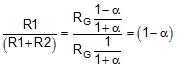
Putting Equation 7 back into the gain expression (Equation 6), and expanding out gives:
Substituting the value of α from Equation 5 into Equation 8 reduces the expression to VO1 = VREF, a gain of 1 V/V. This gain is very precise, as shown in the D2S Electrical Characteristics table, where the tested dc limits are 0.975 V/V to 1.015 V/V.
The D2S output offset and drift are largely determined by the internal elements. The only external consideration is the dc source impedance at the two buffer inputs. With low source impedance, the D2S output offset is tested to be within ±35 mV, that becomes a maximum ±17 mV input differential offset specification. Assuming the dc source impedances are closely matched, the mismatch in the two input bias currents adds another input offset term for higher source impedances. The input bias offset current is limited in test to be < ±0.40 µA. This error term does not rise to add more than ±1 mV input differential offset until the dc source impedance exceeds 2.5 kΩ. A high dc source impedance most commonly occurs in an input ac-coupled, single-supply application, where dc offsets are less critical.
The absolute input bias currents modify the common-mode input voltage if the dc source resistance is too large. The input bias current is tested to a limit of ±4 µA on each input. In order to move the input common-mode voltage by ±100 mV, the dc source impedance must exceed 25 kΩ. This added input common-mode voltage is cancelled by the D2S at the output (pin 6) and is set to the reference voltage applied at VREF (pin 14).
The D2S output noise is largely fixed by the internal elements. The D2S shows a differential input voltage noise of 6 nV/√ Hz, and a current noise of 2 pA/√ Hz on each input. Higher termination resistors increase this source noise, as given by Equation 9, where Rt is the dc termination impedance at each buffer input. The D2S has a 1/f corner at approximately 10 kHz (see Figure 6-18).
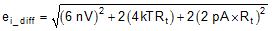
The total differential input noise is dominated by the differential voltage noise. For instance, evaluating this expression for Rt = 200 Ω on each input, increases the total differential input noise to 6.5 nV/√ Hz, only slightly greater than the 6 nV/√ Hz for the D2S with 0 Ω source Rt on each input. If higher final output SNR is desired, consider generating as much input swing as the DAC can support by increasing the termination impedance. It is possible that a lower tail current with higher Rt can yield improved SNR at the D2S input. This differential input noise appears at the D2S output times a gain of 2 V/V.