SBOS780C March 2016 – June 2021 THS3215
PRODUCTION DATA
- 1 Features
- 2 Applications
- 3 Description
- 4 Revision History
- 5 Pin Configuration and Functions
-
6 Specifications
- 6.1 Absolute Maximum Ratings
- 6.2 ESD Ratings
- 6.3 Recommended Operating Conditions
- 6.4 Thermal Information
- 6.5 Electrical Characteristics: D2S
- 6.6 Electrical Characteristics: OPS
- 6.7 Electrical Characteristics: D2S + OPS
- 6.8 Electrical Characteristics: Midscale (DC) Reference Buffer
- 6.9 Typical Characteristics: D2S + OPS
- 6.10 Typical Characteristics: D2S Only
- 6.11 Typical Characteristics: OPS Only
- 6.12 Typical Characteristics: Midscale (DC) Reference Buffer
- 6.13 Typical Characteristics: Switching Performance
- 6.14 Typical Characteristics: Gain Drift
- 7 Parameter Measurement Information
-
8 Detailed Description
- 8.1 Overview
- 8.2 Functional Block Diagram
- 8.3 Feature Description
- 8.4 Device Functional Modes
-
9 Application and Implementation
- 9.1
Application Information
- 9.1.1
Typical Applications
- 9.1.1.1 High-Frequency, High-Voltage, Dual-Output Line Driver for AWGs
- 9.1.1.2 High-Voltage Pulse-Generator
- 9.1.1.3 Single-Supply, AC-Coupled, Piezo Element Driver
- 9.1.1.4 Output Common-Mode Control Using the Midscale Buffer as a Level Shifter
- 9.1.1.5 Differential I/O Driver With independent Common-Mode Control
- 9.1.1
Typical Applications
- 9.1
Application Information
- 10Power Supply Recommendations
- 11Layout
- 12Device and Documentation Support
- 13Mechanical, Packaging, and Orderable Information
Package Options
Mechanical Data (Package|Pins)
- RGV|16
Thermal pad, mechanical data (Package|Pins)
Orderable Information
9.1.1.1.2 Detailed Design Procedure
The THS3215 is well suited for high-speed, low-distortion arbitrary waveform generator (AWG) applications commonly used in laboratory equipment. In this typical application, a high-speed, complementary-current-output DAC is used to drive the D2S. The OPS of the THS3215 easily drives a 50 MHz, 2.5 VPP signal into a matched 50 Ω load. When a larger output signal is required, consider using the THS3095 as the final driver stage.
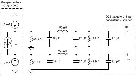
A passive RLC filter is commonly used on DAC outputs to reduce the high-frequency content in the DAC steps. The filtering between the DAC output and the input to the D2S reduces higher-order DAC harmonics from feeding into the internal OPS path when the external input path is selected. Feedthrough between the internal and external OPS paths increases with increasing frequency; however, the input filter rolls off the DAC harmonics before the harmonics couple to VOUT (pin 10) through the deselected OPS signal path. Figure 9-2 shows an example of a doubly-terminated differential filter from the DAC to the THS3215 D2S inputs at +IN (pin 2) and –IN (pin 3). The DAC is modeled as two, fixed, 10 mA currents and a differential, ac-current source. The 10 mA dc midscale currents set up the average common-mode voltage at the DAC outputs and D2S inputs at 10 mA × 25 Ω = 0.25 VCM. The total voltage swing on each DAC output is 0 V to 0.5 V.
 Figure 9-2 105 MHz Butterworth
Filter Between DAC and D2S Inputs
Figure 9-2 105 MHz Butterworth
Filter Between DAC and D2S InputsSome of the guidelines to consider in this filter design are:
- The filter cutoff is adjusted to hit a standard value in the standard high-frequency, chip inductors kits.
- The required filter output capacitance is reduced from the design value of 29.4 pF to 27 pF to account for the D2S input capacitance of 2.4 pF, as reported in the D2S Electrical Characteristics table.
- The capacitor at the DAC output pins must also be reduced by the expected DAC output pin capacitance. The DAC output capacitance is often specified as 5 pF, but is usually much lower. Contact the DAC manufacturer for an accurate value.
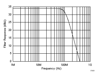
Figure 9-3 shows the TINA-simulated filter response for the input-stage filter. The low-frequency 34 dBΩ gain is due to the 50 Ω differential resistance at the DAC output terminals. At 200 MHz, this filter is down 17 dB from the 50 Ω level; it is also very flat through 50 MHz.
 Figure 9-3 Simulated, Differential-Input Filter Response
In the example design of Figure 9-1, a 50 MHz, third-order Bessel filter is placed between the D2S output and the external OPS input. Another 25 MHz, third-order Bessel filter is placed at the input of a very-high output-swing THS3095 stage. A double-pole, double-throw (DPDT) relay selects the THS3095 path when the internal OPS path is selected in the THS3215. Figure 9-1 shows this design. The key operational considerations in this design include:
- When the external input OPS path is selected, the 2 VPP maximum D2S output swing experiences a 1.55 dB insertion loss from the interstage filter between VO1 (pin 6) and VIN+ (pin 9). A standard value inductor is used and the 464 Ω termination accounts for the internal 18.5 kΩ element. The 10 Ω resistor at VIN+ isolates the OPS input from the 52 pF filter capacitor. To recover the insertion loss and produce a maximum 5 VPP output, the OPS gain is set to 2.96 V/V. When the interstage filter path is selected, the two DPDT relays pass the OPS output on directly from the 49.9 Ω output matching resistor to VO. Disable the THS3095 to conserve power.
- To deliver 20 VPP at the VO output, select the THS3095 path. Select the internal OPS path to bypass the 50 MHz filter (1.55 dB insertion loss) in order to give a maximum 5.9 VPP output at VOUT (pin 11). The two DPDT relays switch position, and the 49.9 Ω at the OPS output becomes part of the 25 MHz, third-order Bessel filter into the THS3095 stage. This filter has a 1 dB insertion loss requiring a gain of 3.8 V/V in the THS3095 to deliver 20 VPP from the OPS output.
- Figure 9-4 and Figure 9-5 show the frequency response and harmonic distortion performance of the dual output-voltage system. The frequency response is normalized to 0 dB to make bandwidth comparisons easier.