SBOS780C March 2016 – June 2021 THS3215
PRODUCTION DATA
- 1 Features
- 2 Applications
- 3 Description
- 4 Revision History
- 5 Pin Configuration and Functions
-
6 Specifications
- 6.1 Absolute Maximum Ratings
- 6.2 ESD Ratings
- 6.3 Recommended Operating Conditions
- 6.4 Thermal Information
- 6.5 Electrical Characteristics: D2S
- 6.6 Electrical Characteristics: OPS
- 6.7 Electrical Characteristics: D2S + OPS
- 6.8 Electrical Characteristics: Midscale (DC) Reference Buffer
- 6.9 Typical Characteristics: D2S + OPS
- 6.10 Typical Characteristics: D2S Only
- 6.11 Typical Characteristics: OPS Only
- 6.12 Typical Characteristics: Midscale (DC) Reference Buffer
- 6.13 Typical Characteristics: Switching Performance
- 6.14 Typical Characteristics: Gain Drift
- 7 Parameter Measurement Information
-
8 Detailed Description
- 8.1 Overview
- 8.2 Functional Block Diagram
- 8.3 Feature Description
- 8.4 Device Functional Modes
-
9 Application and Implementation
- 9.1
Application Information
- 9.1.1
Typical Applications
- 9.1.1.1 High-Frequency, High-Voltage, Dual-Output Line Driver for AWGs
- 9.1.1.2 High-Voltage Pulse-Generator
- 9.1.1.3 Single-Supply, AC-Coupled, Piezo Element Driver
- 9.1.1.4 Output Common-Mode Control Using the Midscale Buffer as a Level Shifter
- 9.1.1.5 Differential I/O Driver With independent Common-Mode Control
- 9.1.1
Typical Applications
- 9.1
Application Information
- 10Power Supply Recommendations
- 11Layout
- 12Device and Documentation Support
- 13Mechanical, Packaging, and Orderable Information
Package Options
Mechanical Data (Package|Pins)
- RGV|16
Thermal pad, mechanical data (Package|Pins)
Orderable Information
8.3.3 Output Power Stage (OPS) (Pins 4, 7, 9, 10, 11, and 12)
A wideband CFA provides a flexible output driver with several unique features. The OPS can be left unused if the specific application only uses the D2S alone, or a combination of the D2S with an off-chip power driver. If left unused, simply tie DISABLE (pin 10) and PATHSEL (pin 4) to the positive supply. This logic configuration turns the OPS off and opens up the external and internal OPS noninverting input paths. An internal fixed 18.5 kΩ resistor holds the external input pin at the logic reference voltage on GND (pin 7). Additionally, the OPS output is connected to the inverting input through another internal 18.5 kΩ resistor when no external resistors are installed on VIN+, VOUT, or VIN– (pins 9, 11, or 12, repectively). Disabling the OPS saves approximately 11 mA of supply current from the nominal total 35 mA, with all stages operating on ±6 V supplies.
The noninverting input to the OPS provides two possible paths controlled by the PATHSEL logic control. With the logic reference (pin 7) at ground, floating PATHSEL or controlling it to a voltage < 0.7 V connects the input path directly to the internal D2S output. Tying PATHSEL to the positive supply, or controlling it to a logic level > 1.3 V, connects the input path to the external input at VIN+. The intent for this switched input is to allow an external filter to be inserted between the D2S output and OPS inputs when needed, and bypass the filter when not. Alternatively, this switched input also allows a completely different signal path to be inserted at the OPS input, independent of that available at the internal D2S output.
In situations where the D2S output at VO1 (pin 6) is switched into another off-chip power driver, the OPS can be disabled using DISABLE. With the logic reference (pin 7) at ground, floating DISABLE, or controlling it to a voltage < 0.7 V, enables the OPS. Tying DISABLE to the positive supply, or controlling it to a logic level > 1.3 V, disables the OPS.
Operation of the wideband, current-feedback OPS requires an external feedback resistor and a gain element. After configuring, the OPS can amplify the D2S output through either the noninverting path, or be configured as an inverting amplifier stage using the external OPS input at VIN+ as a dc reference.
One of the first considerations when designing with the OPS is determining the external resistor values as a function of gain in order to hold the best ac performance. The loop gain (LG) of a CFA is set by the internal open-loop transimpedance gain from the inverting error current to the output, and the effective feedback impedance to the inverting input. The nominal internal open-loop transimpedance gain (ZOL) magnitude and phase are shown in Figure 8-7.
 Figure 8-7 Simulated
OPS ZOL Gain Magnitude and Phase
Figure 8-7 Simulated
OPS ZOL Gain Magnitude and PhaseThe feedback transimpedance (ZOPT) can be approximated as shown in Equation 11, where Ri is the open-loop, high-frequency impedance into the inverting node of the OPS. For a detailed derivation of Equation 11, see the Setting Resistor Values to Optimize Bandwidth section in the OPA695 datasheet (SBOS293).
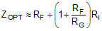
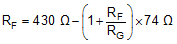
As the signal gain is varied, hold ZOPT approximately constant to hold the ac response constant over gain. Holding ZOPT constant is a requirement to solve for RF. An example of the THS3215 OPS RF derivation is shown in Equation 12:
The calculations are complicated by the internal feedback resistor value of approximately 18.5 kΩ. After the external RF is approximately set by the constant bandwidth consideration, the RG must be set considering the other gain error terms. From the noninverting input of a CFA, the total gain to the output includes a loss through the input buffer stage (described by the CMRR) and the loop gain (LG) loss set by the typical dc open-loop transimpedance gain and the feedback transimpedance. Extract the buffer gain from the VIN+ input to the VIN– input from the CMRR using Equation 13. This gain loss only applies to the noninverting mode of operation and can be ignored in inverting mode operation.
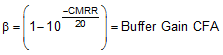
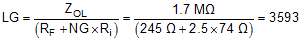
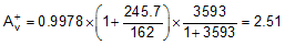
The OPS has a typical CMRR of 53 dB (buffer gain, β = 0.9978) with a tested minimum of 47 dB (minimum buffer gain of 0.9955). The dc LG adds to the gain error. The LG is given by Equation 14, where the typical design gain of 2.5 V/V value is also shown (the 245 Ω shown for RF is the external 249 Ω feedback resistor in parallel with the internal 18.5 kΩ feedback resistor).
The closed-loop output impedance with a heavy load also adds a minor gain loss that is neglected here. The total noninverting gain is then set by Equation 15 (remember to include the internal RF in this analysis). The RF’ shown here is the parallel combination of the internal and external feedback resistors.
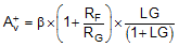
Using nominal values for each term at the specified RF = 249 Ω and RG = 162 Ω gives the gain calculation in Equation 16, yielding a nominal gain very close to 2.5 V/V.
Testing the total gain spread with the internal variation in buffer gain, open-loop transimpedance gain, internal feedback resistor, and ±1% external resistor variation gives a worst-case gain spread of 2.5 V/V to 2.52 V/V. The gain error is primarily dominated by the external 1% resistors. For the tighter tolerance shown in Table 8-1, use 0.1% precision resistors.
At very low gains (< 1.5 V/V), parasitic effects at the inverting input due to stray inductance and capacitance render a flat frequency response impossible. Looking then at gains from 1.5 V/V and up, a table of nominally recommended RF and RG values is shown in Table 8-1. Do not operate the OPS in noninverting gains of less than 2.5 V/V for large output signals because the limited slew-rate of the CFA input buffer causes signal degradation. Table 8-1 accounts for the nominal gain losses described previously, and uses standardized resistor values to minimize the nominal gain-error to target gain. The calculation also restricts the solution to a minimum RG = 20 Ω. The gain calculations include the nominal buffer gain loss, the loop-gain effect, and the nominal internal feedback resistor = 18.5 kΩ.
| TARGET GAIN (V/V) | MEASURED SSBW (MHz) | BEST RF (Ω) |
BEST RG (Ω) |
CALCULATED GAIN | GAIN ERROR (%) | |
|---|---|---|---|---|---|---|
| (V/V) | (dB) | |||||
| 1.5 | 890 | 324 | 634 | 1.498 | 3.513 | -0.1 |
| 2 | — | 287 | 280 | 2.004 | 6.039 | 0.22 |
| 2.5 | 700 | 249 | 162 | 2.510 | 7.995 | 0.41 |
| 3 | — | 205 | 102 | 2.980 | 9.485 | -0.66 |
| 3.5 | — | 169 | 66.5 | 3.510 | 10.905 | 0.27 |
| 4 | — | 150 | 49.9 | 3.972 | 11.980 | -0.7 |
| 4.5 | — | 158 | 44.2 | 4.533 | 13.128 | 0.73 |
| 5 | 390 | 158 | 39.2 | 4.984 | 13.952 | -0.32 |
| 5.5 | — | 165 | 36.5 | 5.467 | 14.755 | -0.6 |
| 6 | — | 169 | 33.2 | 6.029 | 15.605 | 0.49 |
| 6.5 | — | 169 | 30.1 | 6.547 | 16.321 | 0.73 |
| 7 | — | 174 | 28.7 | 6.989 | 16.888 | -0.16 |
| 7.5 | — | 174 | 26.7 | 7.437 | 17.429 | -0.83 |
| 8 | — | 178 | 24.9 | 8.060 | 18.127 | 0.75 |
| 8.5 | — | 178 | 23.2 | 8.578 | 18.668 | 0.92 |
| 9 | — | 178 | 22.1 | 8.955 | 19.041 | -0.5 |
| 9.5 | — | 182 | 21 | 9.558 | 19.608 | 0.61 |
| 10 | 93 | 187 | 20.5 | 10.006 | 20.005 | 0.06 |
The measured bandwidths in Table 8-1 come from Figure 6-25 using the resistor values in the table and a 100 Ω load. Plotting the RF value versus gain gives the curve of Figure 8-8. The curve shows some ripple due to the standard value resistors used to minimize the target dc gain error.
 Figure 8-8 Suggested
External RF Value vs Noninverting Gain for the OPS
Figure 8-8 Suggested
External RF Value vs Noninverting Gain for the OPSUsing RF values greater than the recommended values in Table 8-1 band-limits the response, whereas using less than the recommended RF values peaks the response. Using the values shown in Table 8-1 results in a more constant SSBW (see Figure 6-25. Holding a more constant loop-gain over the external gain setting also acts to hold a more constant output impedance profile, as shown in Figure 8-9. The swept-frequency, closed-loop, output impedance is shown for gains of 2.5 V/V, 5 V/V, and 10 V/V using the RF and RG values of Table 8-1. The first two steps do a good job of delivering the same (and very low) output impedance over frequency, while the gain of 10 V/V shows the expected higher closed-loop output impedance due to the reduced loop-gain and bandwidth.
 Figure 8-9 OPS
Closed-Loop Output Impedance vs Gain Setting
Figure 8-9 OPS
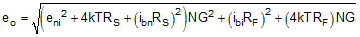
Closed-Loop Output Impedance vs Gain SettingReducing the RF value with increasing gain also helps minimize output noise versus a fixed RF design. See Figure 6-39 for the three noise terms for the OPS. The total output noise calculation is shown in Equation 17:
where
- RS is the source impedance on the noninverting input. If the OPS is driven from the D2S directly using the internal path, RS ≈ 0 Ω.
- NG = (1 + RF / RG) for the design point.
- The flat-band noise numbers for
the OPS are:
- Eni = 2.7 nV/√ Hz
- Ibn = 1.3 pA/√ Hz
- Ibi = 18 pA/√ Hz
Using the values of RF and RG listed in Table 8-1, a swept gain output- and input-referred noise estimate is computed, as shown in Table 8-2. In this sweep, RS = 0 Ω. The input-referred noise (Eni) in Table 8-1 is at the noninverting input of the OPS. To refer the noise to the D2S differential inputs, divide the output noise by two if there is no interstage loss. Dividing the Eni column by 2 V/V shows that the OPS noise contribution is negligible when referred to the D2S inputs, where the 6 nV/√ Hz differential input noise dominates. Operating with higher feedback resistors in the OPS quickly increases the output noise due to the inverting input current noise term. Although increasing RF improves phase margin (for example, when driving a capacitive load), be careful to check the total output noise using Equation 17.
| TARGET GAIN (V/V) |
BEST RF (Ω) |
BEST RG (Ω) |
EO (nV/√ Hz) |
Ein (nV/√ Hz) |
|---|---|---|---|---|
| 1.5 | 324 | 634 | 7.63 | 5.09 |
| 2 | 287 | 280 | 8.07 | 4.03 |
| 2.5 | 249 | 162 | 8.72 | 3.47 |
| 3 | 205 | 102 | 9.39 | 3.15 |
| 3.5 | 169 | 66.5 | 10.42 | 2.97 |
| 4 | 150 | 49.9 | 11.48 | 2.89 |
| 4.5 | 158 | 44.2 | 13.01 | 2.87 |
| 5 | 158 | 39.2 | 14.21 | 2.85 |
| 5.5 | 165 | 36.5 | 15.53 | 2.84 |
| 6 | 169 | 33.2 | 17.04 | 2.83 |
| 6.5 | 169 | 30.1 | 18.42 | 2.81 |
| 7 | 174 | 28.7 | 19.63 | 2.81 |
| 7.5 | 174 | 26.7 | 20.83 | 2.8 |
| 8 | 178 | 24.9 | 22.51 | 2.79 |
| 8.5 | 178 | 23.2 | 23.89 | 2.79 |
| 9 | 178 | 22.1 | 29.41 | 2.78 |
| 9.5 | 182 | 21 | 26.54 | 2.78 |
| 10 | 187 | 20.5 | 27.77 | 2.78 |
Operating the OPS as an inverting amplifier is also possible. When driving the OPS directly from the D2S to the RG resistor, use the values shown in Table 8-1 for the noninverting mode in order to achieve optimal results. Note that the RG resistor is the load for the D2S. Operating with the D2S driving an RG < 80 Ω increases the harmonic distortion of the D2S. In that case, scaling up RF and RG in order to reduce the loading results in better system performance at the cost of a lower OPS bandwidth. In order to reduce layout parasitics, consider splitting the RG resistor in two, with the first half close to VO1 and the second half close to VIN– (pin 12). Splitting RG in this manner places the trace capacitance inside the two resistors, thus keeping both active nodes more stable.
Using the OPS to receive and amplify a signal in the inverting mode with a matched terminating impedance requires another resistor to ground (RM) along with RG. This RM resistor is shown in Figure 8-10 for a 50 Ω matched input impedance design.
 Figure 8-10 Inverting
OPS Operation With Matched Input Impedance
Figure 8-10 Inverting
OPS Operation With Matched Input ImpedanceTable 8-3 gives the recommended external resistor values versus gain for the inverting gain mode with input matching configuration. Table 8-3 solves for the required RF to simultaneously allow the gain, input impedance (50 Ω), and feedback transimpedance to be set to the optimal target values. The table includes the effect of the internal 18.5 kΩ feedback resistor, and minimizes the RMS error to input impedance target (ZI) and overall gain.
| TARGET GAIN —(V/V) |
MEASURED SSBW (MHz) |
BEST RF (Ω) | BEST RG (Ω) | BEST RM (Ω) | CALCULATED GAIN | GAIN ERROR (%) | ZI (Ω) | ZI ERROR (%) | |
|---|---|---|---|---|---|---|---|---|---|
| —(V/V) | (dB) | ||||||||
| 1 | 700 | 294 | 287 | 60.4 | 1.008 | 0.072 | 0.835 | 49.90 | -0.003 |
| 1.5 | — | 267 | 174 | 69.8 | 1.533 | 3.712 | 2.213 | 49.82 | -0.168 |
| 2 | — | 237 | 118 | 86.6 | 2.009 | 6.061 | 0.469 | 49.95 | 0.091 |
| 2.5 | 700 | 226 | 88.7 | 113 | 2.543 | 8.106 | 1.705 | 49.69 | -0.415 |
| 3 | — | 215 | 71.5 | 169 | 3.017 | 9.592 | 0.577 | 50.24 | 0.688 |
| 3.5 | — | 210 | 59 | 316 | 3.553 | 11.011 | 1.508 | 49.72 | -0.366 |
| 4 | — | 205 | 51.1 | 1910 | 4.006 | 12.055 | 0.161 | 49.77 | -0.264 |
| 4.5 | — | 226 | 49.9 | Open | 4.529 | 13.120 | 0.645 | 49.90 | –0.200 |
| 5 | 570 | 249 | 49.9 | Open | 4.990 | 13.962 | -0.201 | 49.90 | –0.200 |
| 5.5 | — | 274 | 49.9 | Open | 5.491 | 14.793 | -0.164 | 49.90 | –0.200 |
| 6 | — | 301 | 49.9 | Open | 6.032 | 15.609 | 0424 | 49.90 | –0.200 |
| 6.5 | — | 324 | 49.9 | Open | 6.493 | 16.249 | -0.108 | 49.90 | –0.200 |
| 7 | — | 348 | 49.9 | Open | 6.974 | 16.870 | -0.372 | 49.90 | –0.200 |
| 7.5 | — | 374 | 49.9 | Open | 7.495 | 17.495 | -0.067 | 49.90 | –0.200 |
| 8 | — | 402 | 49.9 | Open | 8.056 | 18.122 | 0.701 | 49.90 | –0.200 |
| 8.5 | — | 422 | 49.9 | Open | 8.457 | 18.544 | -0.507 | 49.90 | –0.200 |
| 9 | — | 449 | 49.9 | Open | 8.998 | 19.083 | -0.023 | 49.90 | –0.200 |
| 9.5 | — | 475 | 49.9 | Open | 9.519 | 19.572 | 0.200 | 49.90 | –0.200 |
| 10 | 175 | 499 | 49.9 | Open | 10.000 | 20.000 | 0.000 | 49.90 | –0.200 |
At higher gains, RM increases to larger values, and the resistor is excluded from the circuit. The resulting input impedance of the network is resistor RG. From that point, RF simply increases to get higher gains, thereby rapidly reducing the SSBW. However, below a gain of –5 V/V, the inverting design with the values shown in Table 8-3 holds a more constant SSBW versus the noninverting mode (see Figure 6-26).