SBVS151F December   2010  – April 2017 TLV705 , TLV705P

PRODUCTION DATA.  

  1. Features
  2. Applications
  3. Description
  4. Revision History
  5. Pin Configuration and Functions
  6. Specifications
    1. 6.1 Absolute Maximum Ratings
    2. 6.2 ESD Ratings
    3. 6.3 Recommended Operating Conditions
    4. 6.4 Thermal Information
    5. 6.5 Electrical Characteristics
    6. 6.6 Typical Characteristics
  7. Detailed Description
    1. 7.1 Overview
    2. 7.2 Functional Block Diagrams
    3. 7.3 Feature Description
      1. 7.3.1 Internal Current Limit
      2. 7.3.2 Undervoltage Lockout (UVLO)
      3. 7.3.3 Start-Up Current
      4. 7.3.4 Dropout Voltage
      5. 7.3.5 Shutdown
    4. 7.4 Device Functional Modes
      1. 7.4.1 Normal Operation
      2. 7.4.2 Dropout Operation
  8. Application and Implementation
    1. 8.1 Application Information
    2. 8.2 Typical Application
      1. 8.2.1 Design Requirements
      2. 8.2.2 Detailed Design Procedure
        1. 8.2.2.1 Input and Output Capacitor Requirements
        2. 8.2.2.2 Transient Response
      3. 8.2.3 Application Curves
    3. 8.3 Do's and Don'ts
  9. Power Supply Recommendations
  10. 10Layout
    1. 10.1 Layout Guidelines
    2. 10.2 Layout Example
    3. 10.3 Power Dissipation
    4. 10.4 Power Dissipation and Junction Temperature
    5. 10.5 Estimating Junction Temperature
  11. 11Device and Documentation Support
    1. 11.1 Device Support
      1. 11.1.1 Development Support
        1. 11.1.1.1 Evaluation Modules
        2. 11.1.1.2 Spice Models
      2. 11.1.2 Device Nomenclature
    2. 11.2 Documentation Support
      1. 11.2.1 Related Documentation
    3. 11.3 Related Links
    4. 11.4 Community Resources
    5. 11.5 Trademarks
    6. 11.6 Electrostatic Discharge Caution
    7. 11.7 Glossary
  12. 12Mechanical, Packaging, and Orderable Information
    1. 12.1 Package Mounting

Package Options

Mechanical Data (Package|Pins)
Thermal pad, mechanical data (Package|Pins)
Orderable Information

Pin Configuration and Functions

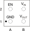
YFF, YFP Packages
4-Pin DSBGA
Top View
TLV705 TLV705P po_bvs151.gif
YFM Package
4-Pin PicoStar
Top View
TLV705 TLV705P po_bvs151.gif

Pin Functions

PIN I/O DESCRIPTION
NAME NO.
GND A1 Ground pin.
EN A2 I Enable pin.
Driving EN over 0.9 V turns on the regulator. Driving EN below 0.4 V places the regulator into shutdown mode, which reduces the operating current to 1 μA (nominal).
VOUT B1 O Regulated output voltage pin.
Placing a small 1-μF ceramic capacitor is required from this pin to ground to ensure stability.
See Input and Output Capacitor Requirements for more details.
VIN B2 I Input pin.
TI recommends placing a small 1-µF capacitor from this pin to ground for good transient performance. See Input and Output Capacitor Requirements for more details.