SBVS322C October 2017 – March 2024 TLV757P
PRODUCTION DATA
- 1
- 1 Features
- 2 Applications
- 3 Description
- 4 Pin Configuration and Functions
- 5 Specifications
- 6 Detailed Description
- 7 Application and Implementation
- 8 Device and Documentation Support
- 9 Revision History
- 10Mechanical, Packaging, and Orderable Information
Package Options
Refer to the PDF data sheet for device specific package drawings
Mechanical Data (Package|Pins)
- DYD|5
- DBV|5
- DRV|6
Thermal pad, mechanical data (Package|Pins)
- DRV|6
Orderable Information
7.1.5.1 Estimating Junction Temperature
The JEDEC standard recommends the use of psi (Ψ) thermal metrics to estimate the junction temperatures of the LDO when in-circuit on a typical PCB board application. These metrics are not thermal resistances, but offer practical and relative means of estimating junction temperatures. These psi metrics are independent of the copper-spreading area. The key thermal metrics (ΨJT and ΨJB) are shown in the Thermal Information table and are used in accordance with Equation 4.
Equation 4. 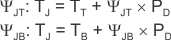
where:
- PD is the power dissipated as shown in Equation 2
- TT is the temperature at the center-top of the device package
- TB is the PCB surface temperature measured 1mm from the device package and centered on the package edge