SLOS498B September   2006  – September 2015 TPA2006D1

PRODUCTION DATA.  

  1. Features
  2. Applications
  3. Description
  4. Revision History
  5. Device Comparison Table
  6. Pin Configuration and Functions
  7. Specifications
    1. 7.1 Absolute Maximum Ratings
    2. 7.2 ESD Ratings
    3. 7.3 Recommended Operating Conditions
    4. 7.4 Thermal Information
    5. 7.5 Electrical Characteristics
    6. 7.6 Operating Characteristics
    7. 7.7 Typical Characteristics
  8. Parameter Measurement Information
  9. Detailed Description
    1. 9.1 Overview
    2. 9.2 Functional Block Diagram
    3. 9.3 Feature Description
      1. 9.3.1 Fully Differential Amplifier
        1. 9.3.1.1 Advantages of Fully Differential Amplifiers
      2. 9.3.2 Efficiency and Thermal Information
      3. 9.3.3 Eliminating the Output Filter With the TPA2006D1 Device
        1. 9.3.3.1 Effect on Audio
        2. 9.3.3.2 Traditional Class-D Modulation Scheme
        3. 9.3.3.3 TPA2006D1 Device Modulation Scheme
        4. 9.3.3.4 Efficiency: Why A Filter is Needed With the Traditional Class-D Modulation Scheme
        5. 9.3.3.5 Effects of Applying a Square Wave into a Speaker
        6. 9.3.3.6 When to Use an Output Filter
      4. 9.3.4 Thermal and Short-Circuit Protection
    4. 9.4 Device Functional Modes
      1. 9.4.1 Summing Input Signals with the TPA2006D1 Device
        1. 9.4.1.1 Summing Two Differential Input Signals
        2. 9.4.1.2 Summing a Differential Input Signal and a Single-Ended Input Signal
        3. 9.4.1.3 Summing Two Single-Ended Input Signals
      2. 9.4.2 Shutdown Mode
  10. 10Application and Implementation
    1. 10.1 Application Information
    2. 10.2 Typical Application
      1. 10.2.1 Design Requirements
      2. 10.2.2 Detailed Design Procedure
        1. 10.2.2.1 Component Selection
        2. 10.2.2.2 Input Resistors (RI)
        3. 10.2.2.3 Decoupling Capacitor (CS)
        4. 10.2.2.4 Input Capacitors (CI)
      3. 10.2.3 Application Curves
    3. 10.3 System Examples
  11. 11Power Supply Recommendations
    1. 11.1 Power Supply Decoupling Capacitors
  12. 12Layout
    1. 12.1 Layout Guidelines
    2. 12.2 Layout Example
  13. 13Device and Documentation Support
    1. 13.1 Community Resources
    2. 13.2 Trademarks
    3. 13.3 Electrostatic Discharge Caution
    4. 13.4 Glossary
  14. 14Mechanical, Packaging, and Orderable Information

Package Options

Mechanical Data (Package|Pins)
Thermal pad, mechanical data (Package|Pins)
Orderable Information

12 Layout

12.1 Layout Guidelines

Place all the external components close to the TPA2006D1 device. The input resistors need to be close to the TPA2006D1 device input pins so noise does not couple on the high impedance nodes between the input resistors and the input amplifier of the TPA2006D1 device. Placing the decoupling capacitor, CS, close to the TPA2006D1 device is important for the efficiency of the class-D amplifier. Any resistance or inductance in the trace between the device and the capacitor can cause a loss in efficiency.

12.2 Layout Example
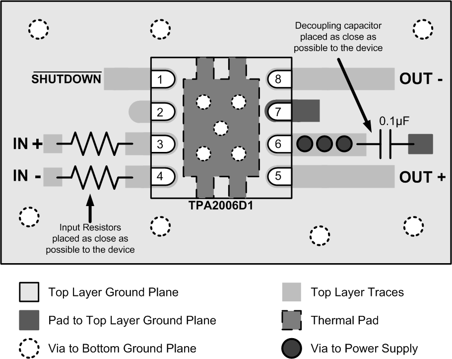
TPA2006D1 layout_QFN_slos498.gif Figure 40. TPA2006D1 Device DRB Package Layout Example