SLOS498B September   2006  – September 2015 TPA2006D1

PRODUCTION DATA.  

  1. Features
  2. Applications
  3. Description
  4. Revision History
  5. Device Comparison Table
  6. Pin Configuration and Functions
  7. Specifications
    1. 7.1 Absolute Maximum Ratings
    2. 7.2 ESD Ratings
    3. 7.3 Recommended Operating Conditions
    4. 7.4 Thermal Information
    5. 7.5 Electrical Characteristics
    6. 7.6 Operating Characteristics
    7. 7.7 Typical Characteristics
  8. Parameter Measurement Information
  9. Detailed Description
    1. 9.1 Overview
    2. 9.2 Functional Block Diagram
    3. 9.3 Feature Description
      1. 9.3.1 Fully Differential Amplifier
        1. 9.3.1.1 Advantages of Fully Differential Amplifiers
      2. 9.3.2 Efficiency and Thermal Information
      3. 9.3.3 Eliminating the Output Filter With the TPA2006D1 Device
        1. 9.3.3.1 Effect on Audio
        2. 9.3.3.2 Traditional Class-D Modulation Scheme
        3. 9.3.3.3 TPA2006D1 Device Modulation Scheme
        4. 9.3.3.4 Efficiency: Why A Filter is Needed With the Traditional Class-D Modulation Scheme
        5. 9.3.3.5 Effects of Applying a Square Wave into a Speaker
        6. 9.3.3.6 When to Use an Output Filter
      4. 9.3.4 Thermal and Short-Circuit Protection
    4. 9.4 Device Functional Modes
      1. 9.4.1 Summing Input Signals with the TPA2006D1 Device
        1. 9.4.1.1 Summing Two Differential Input Signals
        2. 9.4.1.2 Summing a Differential Input Signal and a Single-Ended Input Signal
        3. 9.4.1.3 Summing Two Single-Ended Input Signals
      2. 9.4.2 Shutdown Mode
  10. 10Application and Implementation
    1. 10.1 Application Information
    2. 10.2 Typical Application
      1. 10.2.1 Design Requirements
      2. 10.2.2 Detailed Design Procedure
        1. 10.2.2.1 Component Selection
        2. 10.2.2.2 Input Resistors (RI)
        3. 10.2.2.3 Decoupling Capacitor (CS)
        4. 10.2.2.4 Input Capacitors (CI)
      3. 10.2.3 Application Curves
    3. 10.3 System Examples
  11. 11Power Supply Recommendations
    1. 11.1 Power Supply Decoupling Capacitors
  12. 12Layout
    1. 12.1 Layout Guidelines
    2. 12.2 Layout Example
  13. 13Device and Documentation Support
    1. 13.1 Community Resources
    2. 13.2 Trademarks
    3. 13.3 Electrostatic Discharge Caution
    4. 13.4 Glossary
  14. 14Mechanical, Packaging, and Orderable Information

Package Options

Mechanical Data (Package|Pins)
Thermal pad, mechanical data (Package|Pins)
Orderable Information

8 Parameter Measurement Information

All parameters are measured according to the conditions described in the Specifications section.
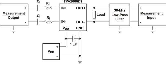
TPA2006D1 tc_test_los498.gif
A. CI is shorted for any common-mode input voltage measurement.
B. A 33-μH inductor is placed in series with the load resistor to emulate a small speaker for efficiency measurements.
C. The 30-kHz low-pass filter is required even if the analyzer has an internal low-pass filter. An RC low-pass filter
(100 Ω, 47 nF) is used on each output for the data sheet graphs.
Figure 27. Test Set-up for Graphs