SLOS498B September   2006  – September 2015 TPA2006D1

PRODUCTION DATA.  

  1. Features
  2. Applications
  3. Description
  4. Revision History
  5. Device Comparison Table
  6. Pin Configuration and Functions
  7. Specifications
    1. 7.1 Absolute Maximum Ratings
    2. 7.2 ESD Ratings
    3. 7.3 Recommended Operating Conditions
    4. 7.4 Thermal Information
    5. 7.5 Electrical Characteristics
    6. 7.6 Operating Characteristics
    7. 7.7 Typical Characteristics
  8. Parameter Measurement Information
  9. Detailed Description
    1. 9.1 Overview
    2. 9.2 Functional Block Diagram
    3. 9.3 Feature Description
      1. 9.3.1 Fully Differential Amplifier
        1. 9.3.1.1 Advantages of Fully Differential Amplifiers
      2. 9.3.2 Efficiency and Thermal Information
      3. 9.3.3 Eliminating the Output Filter With the TPA2006D1 Device
        1. 9.3.3.1 Effect on Audio
        2. 9.3.3.2 Traditional Class-D Modulation Scheme
        3. 9.3.3.3 TPA2006D1 Device Modulation Scheme
        4. 9.3.3.4 Efficiency: Why A Filter is Needed With the Traditional Class-D Modulation Scheme
        5. 9.3.3.5 Effects of Applying a Square Wave into a Speaker
        6. 9.3.3.6 When to Use an Output Filter
      4. 9.3.4 Thermal and Short-Circuit Protection
    4. 9.4 Device Functional Modes
      1. 9.4.1 Summing Input Signals with the TPA2006D1 Device
        1. 9.4.1.1 Summing Two Differential Input Signals
        2. 9.4.1.2 Summing a Differential Input Signal and a Single-Ended Input Signal
        3. 9.4.1.3 Summing Two Single-Ended Input Signals
      2. 9.4.2 Shutdown Mode
  10. 10Application and Implementation
    1. 10.1 Application Information
    2. 10.2 Typical Application
      1. 10.2.1 Design Requirements
      2. 10.2.2 Detailed Design Procedure
        1. 10.2.2.1 Component Selection
        2. 10.2.2.2 Input Resistors (RI)
        3. 10.2.2.3 Decoupling Capacitor (CS)
        4. 10.2.2.4 Input Capacitors (CI)
      3. 10.2.3 Application Curves
    3. 10.3 System Examples
  11. 11Power Supply Recommendations
    1. 11.1 Power Supply Decoupling Capacitors
  12. 12Layout
    1. 12.1 Layout Guidelines
    2. 12.2 Layout Example
  13. 13Device and Documentation Support
    1. 13.1 Community Resources
    2. 13.2 Trademarks
    3. 13.3 Electrostatic Discharge Caution
    4. 13.4 Glossary
  14. 14Mechanical, Packaging, and Orderable Information

Package Options

Mechanical Data (Package|Pins)
Thermal pad, mechanical data (Package|Pins)
Orderable Information

6 Pin Configuration and Functions

VSON Package
8-Pin DRB
Top View
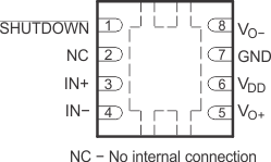
TPA2006D1 po_drb_pckg_top_slos369.gif

Pin Functions

PIN I/O DESCRIPTION
NAME NO.
GND 7 O High-current ground
IN– 4 I Negative differential input
IN+ 3 I Positive differential input
NC 2 No Connect, not connected internal to the device. May be left unconnected.
SHUTDOWN 1 I Shutdown pin (active low logic)
VDD 6 I Power supply
VO+ 5 O Positive BTL output
VO- 8 O Negative BTL output
Thermal Pad Must be soldered to a grounded thermal pad on PCB for best thermal performance.