SLVSB39A December 2011 – June 2014 TPS22929D
PRODUCTION DATA.
- 1 Features
- 2 Applications
- 3 Description
- 4 Simplified Schematic
- 5 Revision History
- 6 Pin Configuration and Functions
- 7 Specifications
- 8 Parametric Measurement Information
- 9 Detailed Description
- 10Application and Implementation
- 11Power Supply Recommendations
- 12Layout
- 13Device and Documentation Support
- 14Mechanical, Packaging, and Orderable Information
Package Options
Mechanical Data (Package|Pins)
- DBV|6
Thermal pad, mechanical data (Package|Pins)
Orderable Information
10 Application and Implementation
10.1 Application Information
10.1.1 VIN to VOUT Voltage Drop
The VIN to VOUT voltage drop in the device is determined by the RON of the device and the load current. The RON of the device depends upon the VIN condition of the device. Refer to the RON specification of the device in the Electrical Characteristics table of this datasheet. Once the RON of the device is determined based upon the VIN conditions, use Equation 1 to calculate the VIN to VOUT voltage drop:
Where,
ΔV = Voltage drop from VIN to VOUT
ILOAD = Load current
RON = On-resistance of the device for a specific VIN
An appropriate ILOAD must be chosen such that the IMAX specification of the device is not violated.
10.1.2 Input Capacitor
To limit the voltage drop on the input supply caused by transient inrush currents, when the switch turns on into a discharged load capacitor or short-circuit, a capacitor needs to be placed between VIN and GND. A 1-μF ceramic capacitor, CIN, placed close to the pins is usually sufficient. Higher values of CIN can be used to further reduce the voltage drop.
10.1.3 Output Capacitor
A CIN to CL ratio of 10 to 1 is recommended for minimizing VIN dip caused by inrush currents during startup.
10.2 Typical Application
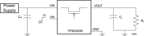 Figure 22. Typical Application Schematic
10.2.1 Design Requirements
| Design Parameter | Example Value |
|---|---|
| VIN | 1.5 V to 5 V |
| CL | 0.1 µF to 1 µF |
| Maximum Acceptable Inrush Current | 10 mA |
10.2.2 Detailed Design Procedure
10.2.2.1 Managing Inrush Current
When the switch is enabled, the output capacitors must be charged up from 0-V to VIN voltage. This charge arrives in the form of inrush current. Inrush current can be calculated using the following equation:
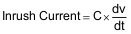
Where,
C = Output capacitance
 = Output slew rate
The TPS22929D offers a very slow controlled rise time for minimizing inrush current. This device can be selected based upon the maximum acceptable slew rate which can be calculated using the design requirements and the inrush current equation. An output capacitance of 1.0 μF will be used since the amount of inrush increases with output capacitance:
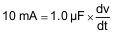

To ensure an inrush current of less than 10 mA, a device with a slew rate less than 10 V/ms must be used.
The TPS22929D has a typical rise time of 4500 μs at 3.3 V . This results in a slew rate of 733 mV/ms which meets the above design requirements.
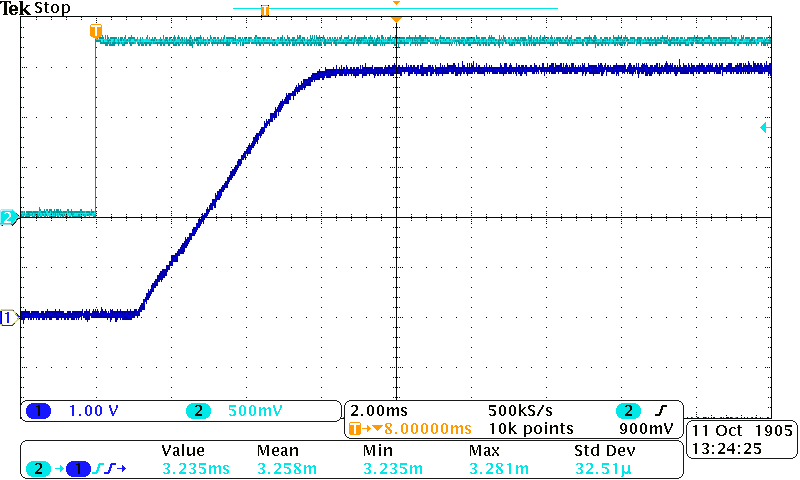
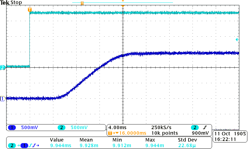
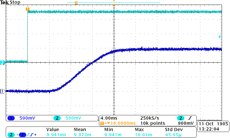
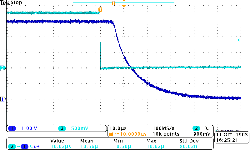
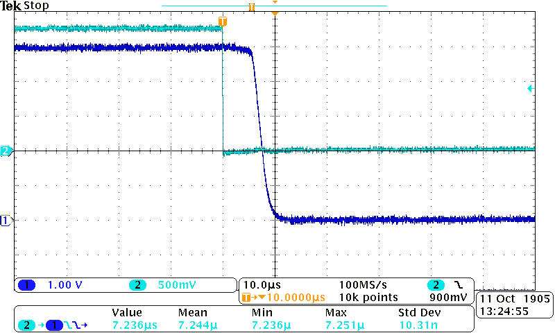
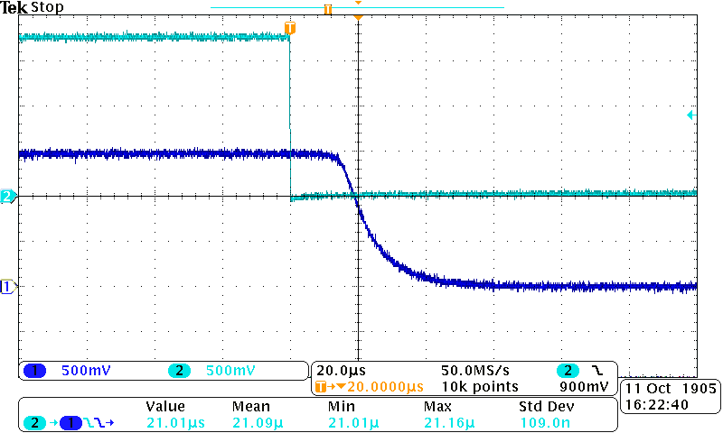
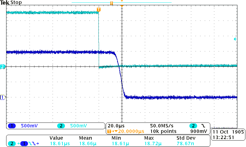
10.2.3 Application Curves
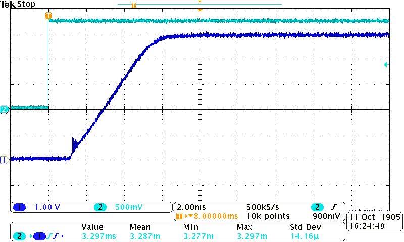
| VIN = 5 V | TA = 25°C | CIN = 10 µF |
| CL = 1 µF | RL = 10 Ω |
| VIN = 5 V | TA = 25°C | CIN = 1 µF |
| CL = 0.1 µF | RL = 10 Ω |
| VIN = 1.5 V | TA = 25°C | CIN = 10 µF |
| CL = 1 µF | RL = 10 Ω | |
| VIN = 1.5 V | TA = 25°C | CIN = 1 µF |
| CL = 0.1 µF | RL = 10 Ω |
| VIN = 5 V | TA = 25°C | CIN = 10 µF |
| CL = 1 µF | RL = 10 Ω |
| VIN = 5 V | TA = 25°C | CIN = 1 µF |
| CL = 0.1 µF | RL = 10 Ω |
| VIN = 1.5 V | TA = 25°C | CIN = 10 µF |
| CL = 1 µF | RL = 10 Ω |
| VIN = 1.5 V | TA = 25°C | CIN = 1 µF |
| CL = 0.1 µF | RL = 10 Ω |