SLVSB39A December 2011 – June 2014 TPS22929D
PRODUCTION DATA.
- 1 Features
- 2 Applications
- 3 Description
- 4 Simplified Schematic
- 5 Revision History
- 6 Pin Configuration and Functions
- 7 Specifications
- 8 Parametric Measurement Information
- 9 Detailed Description
- 10Application and Implementation
- 11Power Supply Recommendations
- 12Layout
- 13Device and Documentation Support
- 14Mechanical, Packaging, and Orderable Information
Package Options
Mechanical Data (Package|Pins)
- DBV|6
Thermal pad, mechanical data (Package|Pins)
Orderable Information
9 Detailed Description
9.1 Overview
The TPS22929D is a single channel, 1.8-A load switch in a small, space-saving 6-pin SOT23-6 package. This devices implement a low resistance P-channel MOSFET with a controlled rise time for applications that need to limit the inrush current.
This device is also designed to have very low leakage current during off state. This prevents downstream circuits from pulling high standby current from the supply. Integrated control logic, driver, power supply, and output discharge FET eliminates the need for additional external components, which reduces solution size and bill of materials (BOM) count.
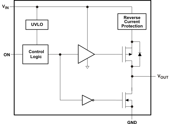
9.2 Functional Block Diagram
9.3 Feature Description
9.3.1 On/Off Control
The ON pin controls the state of the switch. Asserting ON high enables the switch. ON is active high and has a low threshold, making it capable of interfacing with low-voltage signals. The ON pin is compatible with standard GPIO logic threshold. It can be used with any microcontroller with 1.2-V, 1.8-V, 2.5-V or 3.3-V GPIOs.
9.3.2 Output Pull-Down
The output pull-down is active when the user is turning off the main pass FET. The pull-down discharges the output rail to approximately 10% of the rail, and then the output pull-down is automatically disconnected to optimize the shutdown current.
9.3.3 Under-Voltage Lockout
The under-voltage lockout turns-off the switch if the input voltage drops below the under-voltage lockout threshold. During under-voltage lockout (UVLO), if the voltage level at VOUT exceeds the voltage level at VIN by the Reverse Current Voltage Threshold (VRVP), the body diode will be disengaged to prevent any current flow to VIN. With the ON pin active the input voltage rising above the under-voltage lockout threshold will cause a controlled turn-on of the switch which limits current over-shoots.
9.3.4 Reverse Current Protection
In a scenario where VOUT is greater than VIN, there is potential for reverse current through the pass FET or the body diode. The TPS22929D monitors VIN and VOUT voltage levels. When the reverse current voltage threshold (VRVP) is exceeded, the switch is disabled (within 10 µs typ). Additionally, the body diode is disengaged so as to prevent any reverse current flow to VIN. The FET, and the output (VOUT), will resume normal operation when the reverse voltage scenario is no longer present.
Use the following formula to calculate the amount of reverse current required to activate the protection circuit for a particular application:
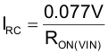
Where,
IRC is the amount of reverse current,
RON(VIN) is the on-resistance as determined by the input voltage.
9.4 Device Functional Modes
Table 1. Function Table
| ON | VIN to VOUT | VOUT to GND(1) |
|---|---|---|
| L | OFF | ON |
| H | ON | OFF |