SLVSB39A December 2011 – June 2014 TPS22929D
PRODUCTION DATA.
- 1 Features
- 2 Applications
- 3 Description
- 4 Simplified Schematic
- 5 Revision History
- 6 Pin Configuration and Functions
- 7 Specifications
- 8 Parametric Measurement Information
- 9 Detailed Description
- 10Application and Implementation
- 11Power Supply Recommendations
- 12Layout
- 13Device and Documentation Support
- 14Mechanical, Packaging, and Orderable Information
Package Options
Mechanical Data (Package|Pins)
- DBV|6
Thermal pad, mechanical data (Package|Pins)
Orderable Information
12 Layout
12.1 Layout Guidelines
For best performance, all traces should be as short as possible. To be most effective, the input and output capacitors should be placed close to the device to minimize the effects that parasitic trace inductances may have on normal operation. Using wide traces for VIN, VOUT, and GND helps minimize the parasitic electrical effects along with minimizing the case to ambient thermal impedance.
12.1.1 Thermal Considerations
For best device performance, be sure to follow the thermal guidelines in the Thermal Information table. To calculate max allowable continuous current for your application for a specific VIN and ambient temperature, use the following formula:
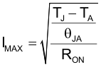
Where:
| IMAX= | Max allowable continuous current |
| TJ= | Max thermal junction temperature (125°C) |
| TA= | Ambient temperature of the application |
| θJA= | Junction-to-air thermal impedance (216°C/W) |
| RON= | RON at a specified input voltage VIN (see Electrical Characteristics) |
12.2 Layout Example
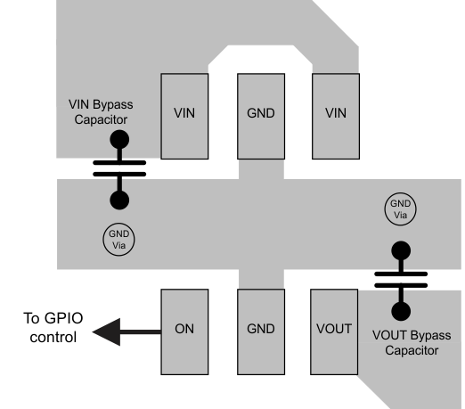 Figure 31. Layout Drawing