SLVSB39A December 2011 – June 2014 TPS22929D
PRODUCTION DATA.
- 1 Features
- 2 Applications
- 3 Description
- 4 Simplified Schematic
- 5 Revision History
- 6 Pin Configuration and Functions
- 7 Specifications
- 8 Parametric Measurement Information
- 9 Detailed Description
- 10Application and Implementation
- 11Power Supply Recommendations
- 12Layout
- 13Device and Documentation Support
- 14Mechanical, Packaging, and Orderable Information
Package Options
Mechanical Data (Package|Pins)
- DBV|6
Thermal pad, mechanical data (Package|Pins)
Orderable Information
7 Specifications
7.1 Absolute Maximum Ratings
over operating free-air temperature range (unless otherwise noted)| MIN | MAX | UNIT | |||
|---|---|---|---|---|---|
| VIN | Input voltage range | –0.3 | 6 | V | |
| VOUT | Output voltage range | –0.3 | 6 | V | |
| VON | Input voltage range | –0.3 | 6 | V | |
| PMAX | Maximum continuous power dissipation at 25°C | 463 | mW | ||
| Maximum continuous power dissipation at 70°C | 254 | ||||
| Maximum continuous power dissipation at 85°C | 185 | ||||
| IMAX | Maximum continuous operating current | 2 | A | ||
| TA | Operating free-air temperature range | –40 | 85 | °C | |
| TJ | Maximum junction temperature | 125 | °C | ||
7.2 Handling Ratings
| MIN | MAX | UNIT | |||
|---|---|---|---|---|---|
| Tstg | Storage temperature range | –65 | 150 | °C | |
| V(ESD) | Electrostatic discharge | Human body model (HBM), per ANSI/ESDA/JEDEC JS-001, all pins(1) | –2 | 2 | kV |
| Charged device model (CDM), per JEDEC specification JESD22-C101, all pins(2) | –1 | 1 | |||
(1) JEDEC document JEP155 states that 500-V HBM allows safe manufacturing with a standard ESD control process. Pins listed as 2 kV may actually have higher performance.
(2) JEDEC document JEP157 states that 250-V CDM allows safe manufacturing with a standard ESD control process. Pins listed as 1 kV may actually have higher performance.
7.3 Recommended Operating Conditions
| MIN | MAX | UNIT | |||
|---|---|---|---|---|---|
| VIN | Input voltage range | 1.4 | 5.5 | V | |
| VON | ON voltage range | 0 | 5.5 | V | |
| VOUT | Output voltage range | VIN | |||
| VIH | High-level input voltage, ON | VIN = 1.4 V to 5.5 V | 1.1 | 5.5 | V |
| VIL | Low-level input voltage, ON | VIN = 3.61 V to 5.5 V | 0.6 | V | |
| VIN = 1.4 V to 3.6 V | 0.4 | V | |||
| CIN | Input Capacitor | 1 (1) | µF | ||
(1) Refer to the application section.
7.4 Thermal Information
| THERMAL METRIC(1) | TPS22929D | UNITS | |
|---|---|---|---|
| DBV | |||
| 6 PINS | |||
| RθJA | Junction-to-ambient thermal resistance | 216 | °C/W |
| RθJCtop | Junction-to-case (top) thermal resistance | 209 | |
| RθJB | Junction-to-board thermal resistance | 131 | |
| ψJT | Junction-to-top characterization parameter | 52 | |
| ψJB | Junction-to-board characterization parameter | 110 | |
(1) For more information about traditional and new thermal metrics, see the IC Package Thermal Metrics application report, SPRA953.
7.5 Electrical Characteristics
VIN = 1.4 V to 5.5 V, TA = –40ºC to 85ºC (unless otherwise noted)| PARAMETER | TEST CONDITIONS | TA | MIN | TYP | MAX | UNIT | |
|---|---|---|---|---|---|---|---|
| IIN | Quiescent current | IOUT = 0, VIN = VON = 5.25 V | Full | 2.2 | 10 | µA | |
| IOUT = 0, VIN = VON = 4.2 V | 2.1 | 7.0 | |||||
| IOUT = 0, VIN = VON = 3.6 V | 2.0 | 7.0 | |||||
| IOUT = 0, VIN = VON = 2.5 V | 1.0 | 5.0 | |||||
| IOUT = 0, VIN = VON = 1.5 V | 0.8 | 5.0 | |||||
| IIN(off) | Off supply current | VON = GND, VOUT = Open, VIN = 5.25 V | Full | 0.8 | 10 | µA | |
| VON = GND, VOUT = Open, VIN = 4.2 V | 0.3 | 7.0 | |||||
| VON = GND, VOUT = Open, VIN = 3.6 V | 0.2 | 7.0 | |||||
| VON = GND, VOUT = Open, VIN = 2.5 V | 0.2 | 5.0 | |||||
| VON = GND, VOUT = Open, VIN = 1.5 V | 0.1 | 5.0 | |||||
| IIN(Leakage) | Leakage current | VON = GND, VOUT = 0, VIN = 5.25 V | Full | 0.8 | 10 | µA | |
| VON = GND, VOUT = 0, VIN = 4.2 V | 0.3 | 7.0 | |||||
| VON = GND, VOUT = 0, VIN = 3.6 V | 0.2 | 7.0 | |||||
| VON = GND, VOUT = 0, VIN = 2.5 V | 0.2 | 5.0 | |||||
| VON = GND, VOUT = 0, VIN = 1.5 V | 0.1 | 5.0 | |||||
| rON | On-resistance | VIN = 5.25 V, IOUT = –200 mA | 25°C | 115 | 150 | mΩ | |
| Full | 175 | ||||||
| VIN = 5.0 V, IOUT = –200 mA | 25°C | 115 | 150 | ||||
| Full | 175 | ||||||
| VIN = 4.2 V, IOUT = –200 mA | 25°C | 115 | 150 | ||||
| Full | 175 | ||||||
| VIN = 3.3 V, IOUT = –200 mA | 25°C | 115 | 150 | ||||
| Full | 175 | ||||||
| VIN = 2.5 V, IOUT = –200 mA | 25°C | 118 | 155 | ||||
| Full | 180 | ||||||
| VIN = 1.5 V, IOUT = –200 mA | 25°C | 129 | 170 | ||||
| Full | 200 | ||||||
| RPD | Output pull down resistance | VIN = 3.3 V, VON = 0, IOUT = 30 mA | 25°C | 150 | 200 | Ω | |
| UVLO | Under voltage lockout | VIN increasing, VON = 3.6 V, IOUT = –100 mA |
Full | 1.4 | V | ||
| VIN decreasing, VON 3.6 V, RL = 10 Ω | 0.50 | ||||||
| ION | ON input leakage current | VON = 1.4 V to 5.25 V or GND | Full | 1 | µA | ||
| VRVP | Reverse Current Voltage Threshold | 77 | mV | ||||
| tDELAY | Reverse Current Response Delay | VIN = 5V | 10 | µs | |||
7.6 Switching Characteristics
| PARAMETER | TEST CONDITION | TPS22929D | UNIT | |
|---|---|---|---|---|
| TYP | ||||
| VIN = 5 V, TA = 25ºC (unless otherwise noted) | ||||
| tON | Turn-ON time | RL = 10 Ω, CL = 0.1 µF | 3315 | µs |
| tOFF | Turn-OFF time | RL = 10 Ω, CL = 0.1 µF | 7.4 | |
| tR | VOUT rise time | RL = 10 Ω, CL = 0.1 µF | 3660 | |
| tF | VOUT fall time | RL = 10 Ω, CL = 0.1 µF | 6.1 | |
| VIN = 3.3 V, TA = 25ºC (unless otherwise noted) | ||||
| tON | Turn-ON time | RL = 10 Ω, CL = 0.1 µF | 4655 | µs |
| tOFF | Turn-OFF time | RL = 10 Ω, CL = 0.1 µF | 9.5 | |
| tR | VOUT rise time | RL = 10 Ω, CL = 0.1 µF | 4150 | |
| tF | VOUT fall time | RL = 10 Ω, CL = 0.1 µF | 3.0 | |
| VIN = 1.5 V, TA = 25ºC (unless otherwise noted) | ||||
| tON | Turn-ON time | RL = 10 Ω, CL = 0.1 µF | 10175 | µs |
| tOFF | Turn-OFF time | RL = 10 Ω, CL = 0.1 µF | 18.3 | |
| tR | VOUT rise time | RL = 10 Ω, CL = 0.1 µF | 7812 | |
| tF | VOUT fall time | RL = 10 Ω, CL = 0.1 µF | 3.0 | |
7.7 Typical Characteristics
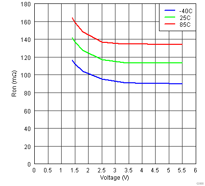 Figure 1. On-State Resistance vs Input Voltage
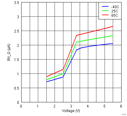 Figure 3. Input Current, Quiescent vs Input Voltage
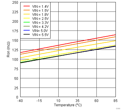 Figure 5. On-State Resistance vs Temperature
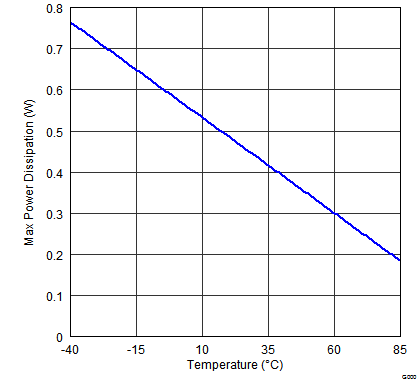 Figure 7. Allowable Power Dissipation
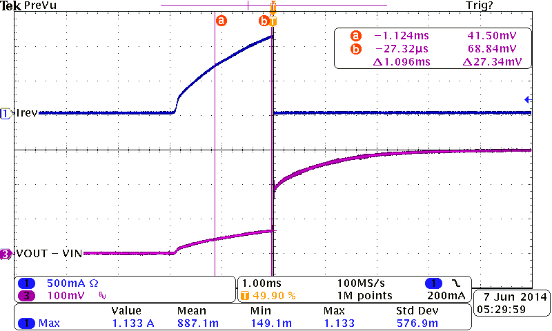 Figure 9. Reverse Current Protection (VIN = 3.0 V, VOUT Ramp up From 3.0 V to 3.3 V)
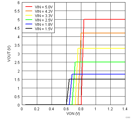 Figure 2. On Input Threshold
 Figure 4. Input Current, Leak vs Input Voltage
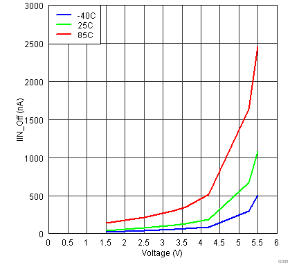 Figure 6. Input Current, Off vs Input Voltage
(IOUT = –100mA)
7.7.1 Typical AC Characteristics
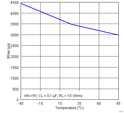 Figure 10. Rise Time vs Temperature
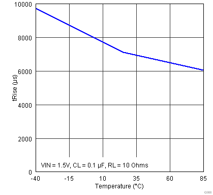 Figure 12. Rise Time vs Temperature
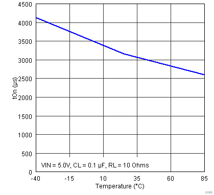 Figure 14. Turn-On Time vs Temperature
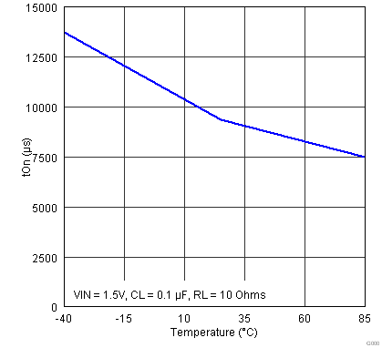 Figure 16. Turn-On Time vs Temperature
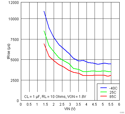 Figure 18. Rise Time vs Input Voltage
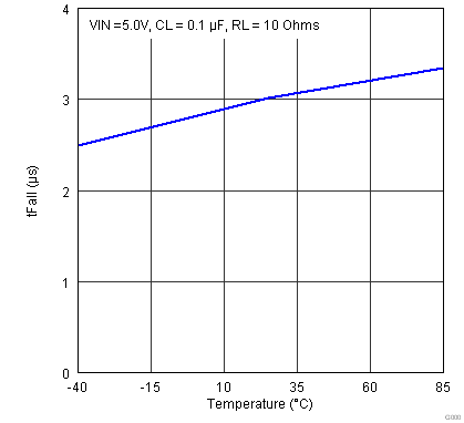 Figure 11. Fall Time vs Temperature
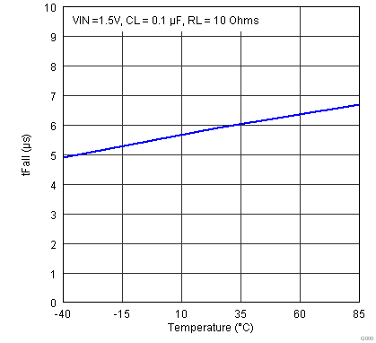 Figure 13. Fall Time vs Temperature
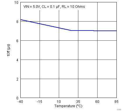 Figure 15. Turn-Off Time vs Temperature
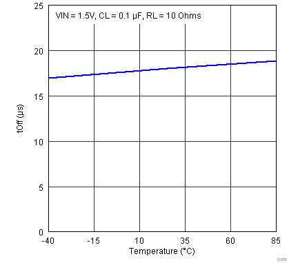 Figure 17. Turn-Off Time vs Temperature
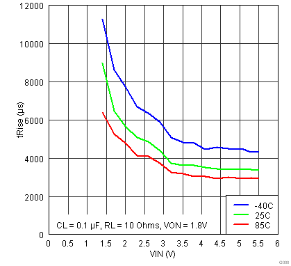 Figure 19. Rise Time vs Input Voltage