SLUSD62 December 2017 TPS40345
PRODUCTION DATA.
- 1 Features
- 2 Applications
- 3 Description
- 4 Revision History
- 5 Pin Configuration and Functions
- 6 Specifications
- 7 Detailed Description
-
8 Application and Implementation
- 8.1 Application Information
- 8.2
Typical Applications
- 8.2.1 Design Requirements
- 8.2.2
Detailed Design Procedure
- 8.2.2.1 Selecting the Switching Frequency
- 8.2.2.2 Inductor Selection (L1)
- 8.2.2.3 Output Capacitor Selection (C12)
- 8.2.2.4 Peak Current Rating of Inductor
- 8.2.2.5 Input Capacitor Selection (C8)
- 8.2.2.6 MOSFET Switch Selection (Q1 and Q2)
- 8.2.2.7 Bootstrap Capacitor (C6)
- 8.2.2.8 VDD Bypass Capacitor (C7)
- 8.2.2.9 BP Bypass Capacitor (C5)
- 8.2.2.10 Short-Circuit Protection (R11)
- 8.2.2.11 Feedback Divider (R4, R5)
- 8.2.2.12 Compensation: (C2, C3, C4, R3, R6)
- 8.2.3 Application Curves
- 9 Power Supply Recommendations
- 10Layout
- 11Device and Documentation Support
- 12Mechanical, Packaging, and Orderable Information
Package Options
Mechanical Data (Package|Pins)
- DRC|10
Thermal pad, mechanical data (Package|Pins)
- DRC|10
Orderable Information
8 Application and Implementation
NOTE
Information in the following applications sections is not part of the TI component specification, and TI does not warrant its accuracy or completeness. TI’s customers are responsible for determining suitability of components for their purposes. Customers should validate and test their design implementation to confirm system functionality.
8.1 Application Information
The TPS40345 a cost-optimized synchronous buck controllers providing high-end features to construct high-performance DC-DC converters. Prebias capability eliminates concerns about damaging sensitive loads during start-up. Programmable overcurrent protection levels and hiccup overcurrent fault recovery maximize design flexibility and minimize power dissipation in the event of a prolonged output short. frequency spread spectrum (FSS) feature reduces peak EMI noise by spreading the initial energy of each harmonic along a frequency band, thus giving a wider spectrum with lower amplitudes.
8.2 Typical Applications
For this 20-A, 12-V to 1.2-V design, the 600-kHz TPS40345 was selected for a balance between small size and high efficiency.
 Figure 12. TPS40345 Design Example Schematic
8.2.1 Design Requirements
For this example, follow the design parameters listed in Table 1.
Table 1. Design Example Electrical Characteristics
| PARAMETER | TEST CONDITIONS | MIN | TYP | MAX | UNIT | ||
|---|---|---|---|---|---|---|---|
| VIN | Input voltage | 8 | 14 | V | |||
| VINripple | Input ripple | IOUT = 20 A | 0.5 | V | |||
| VOUT | Output voltage | 0 A ≤ IOUT ≤ 20 A | 1.164 | 1.2 | 1.236 | V | |
| Line regulation | 8 V ≤ VIN ≤ 14 V | 0.5% | |||||
| Load regulation | 0 A ≤ IOUT ≤ 20 A | 0.5% | |||||
| VRIPPLE | Output ripple | IOUT = 20 A | 36 | mV | |||
| VOVER | Output overshoot | 5 A ≤ IOUT ≤ 15 A | 100 | mV | |||
| VUNDER | Output undershoot | 5 A ≤ IOUT ≤ 15 A | 100 | mV | |||
| IOUT | Output current | 8 V ≤ VIN ≤ 14 V | 0 | 20 | A | ||
| tSS | Soft-start time | VIN = 12 V | 1.5 | ms | |||
| ISCP | Short-circuit current trip point | 26 | A | ||||
| fSW | Switching frequency | 600 | kHz | ||||
| Size | 1.5 | in2 | |||||
8.2.2 Detailed Design Procedure
8.2.2.1 Selecting the Switching Frequency
To achieve the small size for this design the TPS40345, with fSW = 600 kHz, is selected for minimal external component size.
8.2.2.2 Inductor Selection (L1)
Synchronous buck power inductors are typically sized for approximately 30% peak-to-peak ripple current (IRIPPLE).
Given this target ripple current, the required inductor size can be calculated in Equation 3.

Selecting a standard 300-nH inductor value, solve for IRIPPLE = 6 A
The RMS current through the inductor is approximated by Equation 4.

8.2.2.3 Output Capacitor Selection (C12)
The selection of the output capacitor is typically driven by the output transient response. Equation 5 and Equation 6 overestimate the voltage deviation to account for delays in the loop bandwidth and can be used to determine the required output capacitance.


If VIN(min) > 2 × VOUT, use overshoot (Equation 5) to calculate minimum output capacitance. If VIN(min) < 2 × VOUT, use undershoot (Equation 6) to calculate minimum output capacitance.

With a minimum capacitance, the maximum allowable ESR is determined by the maximum ripple voltage and is approximated by Equation 8.

Two 47-µF and one 220-µF capacitors are selected to provide more than 250 µF of minimum capacitance and 5.2 mΩ of ESR.
8.2.2.4 Peak Current Rating of Inductor
With output capacitance, it is possible to calculate the charge current during start-up and determine the minimum saturation current rating for the inductor. The start-up charging current is approximated by Equation 9.


Table 2. Inductor Requirements
| PARAMETER | VALUE | UNIT | |
|---|---|---|---|
| L | Inductance | 300 | nH |
| IL(rms) | RMS current (thermal rating) | 20.07 | A |
| IL(peak) | Peak current (saturation rating) | 23.25 | A |
8.2.2.5 Input Capacitor Selection (C8)
The input voltage ripple is divided between capacitance and ESR. For this design VRIPPLE(cap) = 150 mV and VRIPPLE(esr) = 150 mV. The minimum capacitance and maximum ESR are estimated by Equation 11.


The RMS current in the input capacitors is estimated by Equation 13.

Three 1210, 10-µF, 25-V, X5R ceramic capacitors are selected. Higher voltage capacitors are selected to minimize capacitance loss at the DC bias voltage to ensure the capacitors allow sufficient capacitance at the working voltage.
8.2.2.6 MOSFET Switch Selection (Q1 and Q2)
Reviewing available TI NexFET MOSFETs using the TI NexFET MOSFET selection tool, the CSD16410Q5A and CSD16321Q5 5-mm × 6-mm MOSFETs are selected.
These two FETs have maximum total gate charges of 5 nC and 10 nC, respectively.
8.2.2.7 Bootstrap Capacitor (C6)
To ensure proper charging of the high-side FET gate, limit the ripple voltage on the boost capacitor to less than 50 mV.

8.2.2.8 VDD Bypass Capacitor (C7)
Per this TPS40345 data sheet, select a 1-uF X5R or better ceramic bypass capacitor for VDD.
8.2.2.9 BP Bypass Capacitor (C5)
Per the TPS40345 data sheet, a minimum 1-uF ceramic capacitance is required to stabilize the BP regulator. To limit regulator noise to less than 10 mV, the value of the bypass capacitor is calculated in Equation 15.

Because Q2 is larger than Q1, and the total gate charge of Q2 is 10 nC, a BP capacitor of 1 µF is calculated. A standard value of 1 µF is selected to limit noise on the BP regulator.
8.2.2.10 Short-Circuit Protection (R11)
The TPS40345 uses the negative drop across the low-side FET at the end of the OFF-time to measure the inductor current. Allowing for 30% over maximum load and 20% rise in RDS(on)Q1 for self-heating, the voltage drop across the low-side FET at current limit is given by Equation 16.

The TPS40345 internal temperature coefficient helps compensate for the MOSFET’s RDS(on) temperature coefficient, so the current limit programming resistor is selected by Equation 17.

8.2.2.11 Feedback Divider (R4, R5)
The TPS40345 controller uses a full operational amplifier with an internally fixed 0.6-V reference. R4 is selected between 10 kΩ and 50 kΩ for a balance of feedback current and noise immunity. With R4 set to 10 kΩ, The output voltage is programmed with a resistor divider given by Equation 18.

8.2.2.12 Compensation: (C2, C3, C4, R3, R6)
Using the TPS40k Loop Stability Tool for 100-kHz bandwidth and 60° phase margin with a R4 value of 10.0 kΩ, the following values are returned.
- C4 = 680 pF
- C5 = 100 pF
- C6 = 680 pF
- R1 = 10 kΩ
- R2 = 1.5 kΩ
8.2.3 Application Curves

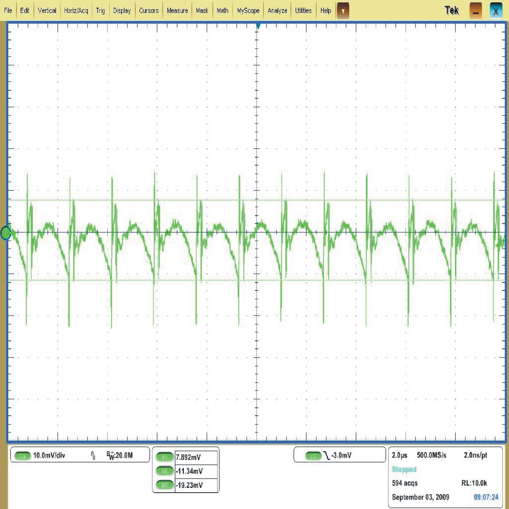
 Figure 15. Output Ripple 10 mV/div, 2-µs/div, 20-MHz Bandwidth
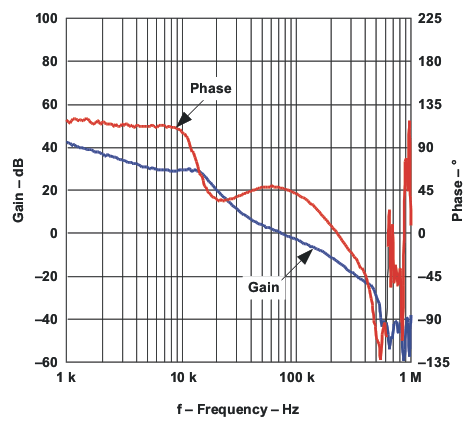
 Figure 14. Gain and Phase vs Frequency