SLUSD62 December 2017 TPS40345
PRODUCTION DATA.
- 1 Features
- 2 Applications
- 3 Description
- 4 Revision History
- 5 Pin Configuration and Functions
- 6 Specifications
- 7 Detailed Description
-
8 Application and Implementation
- 8.1 Application Information
- 8.2
Typical Applications
- 8.2.1 Design Requirements
- 8.2.2
Detailed Design Procedure
- 8.2.2.1 Selecting the Switching Frequency
- 8.2.2.2 Inductor Selection (L1)
- 8.2.2.3 Output Capacitor Selection (C12)
- 8.2.2.4 Peak Current Rating of Inductor
- 8.2.2.5 Input Capacitor Selection (C8)
- 8.2.2.6 MOSFET Switch Selection (Q1 and Q2)
- 8.2.2.7 Bootstrap Capacitor (C6)
- 8.2.2.8 VDD Bypass Capacitor (C7)
- 8.2.2.9 BP Bypass Capacitor (C5)
- 8.2.2.10 Short-Circuit Protection (R11)
- 8.2.2.11 Feedback Divider (R4, R5)
- 8.2.2.12 Compensation: (C2, C3, C4, R3, R6)
- 8.2.3 Application Curves
- 9 Power Supply Recommendations
- 10Layout
- 11Device and Documentation Support
- 12Mechanical, Packaging, and Orderable Information
Package Options
Mechanical Data (Package|Pins)
- DRC|10
Thermal pad, mechanical data (Package|Pins)
- DRC|10
Orderable Information
10 Layout
10.1 Layout Guidelines
- For MOSFET or power block layout, follow the layout recommendations provided for the MOSFET or power block selected.
- Connect VDD to VIN as close as possible to the drain connection of the high-side FET to avoid introducing additional drop, which could trigger short-circuit protection.
- Place VDD and BP to GND capacitors within 2 mm of the device and connected to the thermal pad (GND).
- Connect the FB to GND resistor to the thermal tab (GND) with a minimum 10-mil wide trace.
- Place VOUT to FB resistor within 2 mm of the FB pin.
- Connect the EN/SS-to-GND capacitor to the thermal tab (GND) with a minimum 10-mil-wide trace. It may share this trace with FB to GND.
- If a BJT or MOSFET is used to disable EN/SS, place it within 5 mm of the device.
- If a COMP to GND resistor is used, place it within 5 mm of the device.
- All COMP and FB traces should be kept minimum line width and as short as possible to minimize noise coupling.
- EN/SS should not be routed more than 20 mm from the device.
- If multiple layers are used, extend GND under all components connected to FB, COMP and EN/SS to reduce noise sensitivity.
- HDRV and LDRV must provide short, low inductance paths of 5 mm or less to the gates of the MOSFETs or power block.
- Place no more than 1 Ω of resistance between HDRV or LDRV and their MOSFET or power block gate pins.
- LDRV / OC to GND current limit programming resistor may be placed on the far side of the MOSFET if necessary to ensure a short connection from LDRV to the gate of the low-side MOSFET.
- Place the BOOT to SW resistor and capacitor within 4 mm of the device using a minimum of 10-mil-wide trace. The full width of the component pads are preferred for trace widths if design rules allow.
- If via must be used between the HDRV, SW and LDRV pins and their respective MOSFET or power block connections, use a minimum of two vias to reduce parasitic inductance
- Refer to the land pattern data for the preferred layout of thermal vias within the thermal pad.
- TI recommends extending the top-layer copper area of the thermal pad (GND) beyond the package a minimum 3 mm between pins 1 and 10 and 5 and 6 to improve thermal resistance to ambient of the device.
10.2 Layout Example
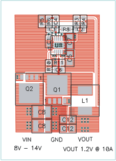
 Figure 16. Top Copper With Components
..
..
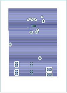
 Figure 18. Bottom Internal Copper Layout
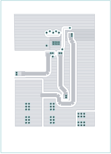
 Figure 17. Top Internal Copper Layout
..
..
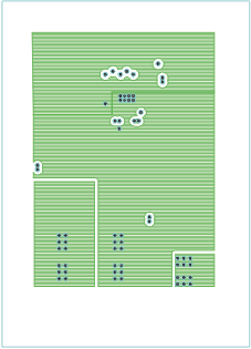
 Figure 19. Bottom Copper Layer