SLUSD62 December 2017 TPS40345
PRODUCTION DATA.
- 1 Features
- 2 Applications
- 3 Description
- 4 Revision History
- 5 Pin Configuration and Functions
- 6 Specifications
- 7 Detailed Description
-
8 Application and Implementation
- 8.1 Application Information
- 8.2
Typical Applications
- 8.2.1 Design Requirements
- 8.2.2
Detailed Design Procedure
- 8.2.2.1 Selecting the Switching Frequency
- 8.2.2.2 Inductor Selection (L1)
- 8.2.2.3 Output Capacitor Selection (C12)
- 8.2.2.4 Peak Current Rating of Inductor
- 8.2.2.5 Input Capacitor Selection (C8)
- 8.2.2.6 MOSFET Switch Selection (Q1 and Q2)
- 8.2.2.7 Bootstrap Capacitor (C6)
- 8.2.2.8 VDD Bypass Capacitor (C7)
- 8.2.2.9 BP Bypass Capacitor (C5)
- 8.2.2.10 Short-Circuit Protection (R11)
- 8.2.2.11 Feedback Divider (R4, R5)
- 8.2.2.12 Compensation: (C2, C3, C4, R3, R6)
- 8.2.3 Application Curves
- 9 Power Supply Recommendations
- 10Layout
- 11Device and Documentation Support
- 12Mechanical, Packaging, and Orderable Information
Package Options
Mechanical Data (Package|Pins)
- DRC|10
Thermal pad, mechanical data (Package|Pins)
- DRC|10
Orderable Information
7 Detailed Description
7.1 Overview
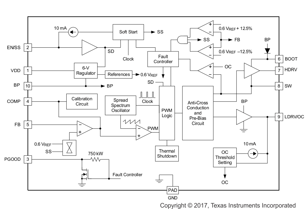
The TPS40345 is a cost-optimized synchronous buck controller providing high-end features to construct high-performance DC–DC converters. Prebias capability eliminates concerns about damaging sensitive loads during start-up. Programmable overcurrent protection levels and hiccup overcurrent fault recovery maximize design flexibility and minimize power dissipation in the event of a prolonged output short. The frequency spread spectrum (FSS) feature reduces peak EMI noise by spreading the initial energy of each harmonic along a frequency band, thus giving a wider spectrum with lower amplitudes.
7.2 Functional Block Diagram

7.3 Feature Description
7.3.1 Voltage Reference
The 600-mV bandgap cell is internally connected to the noninverting input of the error amplifier. The reference voltage is trimmed with the error amplifier in a unity gain configuration to remove amplifier offset from the final regulation voltage. The 1.3% tolerance on the reference voltage allows the user to design a very accurate power supply.
7.3.2 Enable Functionality, Start-Up Sequence and Timing
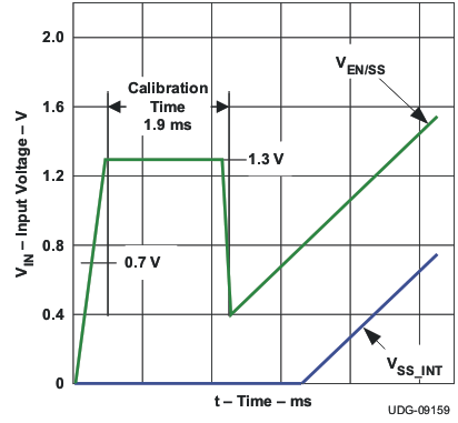
After input power is applied, an internal current source of 40 µA starts to charge up the soft-start capacitor connected from EN/SS to GND. When the voltage across that capacitor increases to 0.7 V, it enables the internal BP regulator followed by a calibration. The total calibration time is about 1.9 ms. See Figure 11. During the calibration, the device performs in the following way. It disables the LDRV drive and injects an internal 10-µA current source to the resistor connected from LDRV to GND. The voltage developed across that resistor is then sampled and latched internally as the OCP trip level until one cycles the input or toggles the EN/SS.
 Figure 11. Start-Up Sequence and Timing
The voltage at EN/SS is internally clamped to 1.3 V before and/or during calibration to minimize the discharging time once calibration. The discharging current is from an internal current source of 140 µA and it pulls the voltage down to 0.4 V. The discharging current then initiates the soft-start by charging up the capacitor using an internal current source of 10 µA. The resulting voltage ramp on this pin is used as a second noninverting input to the error amplifier after an 800 mV (typical) downward level-shift; therefore, actual soft-start does not occur until the voltage at this pin reaches 800 mV.
If EN/SS is left floating, the controller starts automatically. EN/SS must be pulled down to less than 270 mV to ensure that the chip is in shutdown mode.
7.3.3 Soft-Start Time
The soft-start time of the TPS40345 is user programmable by selecting a single capacitor. The EN/SS pin sources 10 µA to charge this capacitor. The actual output ramp-up time is the amount of time that it takes for the 10 µA to charge the capacitor through a 600-mV range. There is some initial lag due to calibration and an offset (800 mV) from the actual EN/SS pin voltage to the voltage applied to the error amplifier.
The soft-start is done in a closed-loop fashion, meaning that the error amplifier controls the output voltage at all times during the soft-start period and the feedback loop is never open as occurs in duty cycle limit soft-start schemes. The error amplifier has two non-inverting inputs, one connected to the 600-mV reference voltage, and the other connected to the offset EN/SS pin voltage. The lower of these two voltages is what the error amplifier controls the FB pin. As the voltage on the EN/SS pin ramps up past approximately 1.4 V (800-mV offset voltage plus the 600 mV reference voltage), the 600-mV reference voltage becomes the dominant input and the converter has reached its final regulation voltage.
The capacitor required for a given soft-start ramp time for the output voltage is given by Equation 1.

where
- CSS is the required capacitance on the EN/SS pin. (F)
- ISS is the soft-start source current (10 µA).
- VFB is the feedback reference voltage (0.6 V).
- tSS is the desired soft-start ramp time (s).
7.3.4 Oscillator and Frequency Spread Spectrum (FSS)
The oscillator frequency is internally fixed. The TPS40345 operating frequency is 600 kHz.
Connecting a resistor with a value of 267 kΩ ±10% from BP to EN/SS enables the FSS feature. When the FSS is enabled, it spreads the internal oscillator frequency over a minimum 12% window using a 25-kHz modulation frequency with triangular profile. By modulating the switching frequency, side-bands are created. The emission power of the fundamental switching frequency and its harmonics is distributed into smaller pieces scattered around many sideband frequencies. The effect significantly reduces the peak EMI noise and makes it much easier for the resultant emission spectrum to pass EMI regulations.
7.3.5 Overcurrent Protection
Programmable OCP level at LDRV is from 6 mV to 150 mV at room temperature with 3000 ppm temperature coefficient to help compensate for changes in the low-side FET channel resistance as temperature increases. With a scale factor of 2, the actual trip point across the low-side FET is in the range of 12 mV to 300 mV. The accuracy of the internal current source is ±5%. Overall offset voltage, including the offset voltage of the internal comparator and the amplifier for scale factor of 2, is limited to ±8 mV.
Maximum clamp voltage at LDRV is 340 mV to avoid turning on the low-side FET during calibration and in a prebiased condition. The maximum clamp voltage is fixed and it does not change with temperature. If the voltage drop across ROCSET reaches the 340-mV maximum clamp voltage during calibration (no ROCSET resistor included), it disables OC protection. Once disabled, there is no low-side or high-side current sensing.
OCP level at HDRV is fixed at 450 mV with 3000-ppm temperature coefficient to help compensate for changes in the high-side FET channel resistance as temperature increases. OCP at HDRV provides pulse-by-pulse current limiting.
OCP sensing at LDRV is a true inductor valley current detection, using sample and hold. Equation 2 can be used to calculate ROCSET:

where
- IOCSET is the internal current source.
- VOCLOS is the overall offset voltage.
- IP-P is the peak-to-peak inductor current.
- RDS(on) is the drain to source ON-resistance of the low-side FET.
- IOUT(max) is the trip point for OCP.
- ROCSET is the resistor used for setting the OCP level.
To avoid overcurrent tripping in normal operating load range, calculate ROCSET using Equation 2 with:
- The maximum RDS(ON) at room temperature
- The lower limit of VOCLOS (–8 mV) and the lower limit of IOCSET (9.5 µA) from the Electrical Characteristics table.
- The peak-to-peak inductor current IP-P at minimum input voltage
Overcurrent is sensed across both the low-side FET and the high-side FET. If the voltage drop across either FET exceeds the OC threshold, a count increments one count. If no OC is detected on either FET, the fault counter decrements by one count. If three OC pulses are summed, a fault condition is declared which cycles the soft-start function in a hiccup mode. Hiccup mode consists of four dummy soft-start timeouts followed by a real one if overcurrent condition is encountered during normal operation, or five dummy soft-start timeouts followed by a real one if overcurrent condition occurs from the beginning during start. This cycle continues indefinitely until the fault condition is removed.
7.3.6 Drivers
The drivers for the external high-side and low-side MOSFETs can drive a gate-to-source voltage of VBP. The LDRV driver for the low-side MOSFET switches between BP and GND, while the HDRV driver for the high-side MOSFET is referenced to SW and switches between BOOT and SW. The drivers have nonoverlapping timing that is governed by an adaptive delay circuit to minimize body diode conduction in the synchronous rectifier.
7.3.7 Prebias Start-Up
The TPS40345 contains a circuit to prevent current from being pulled from the output during start-up in the condition the output is prebiased. There are no PWM pulses until the internal soft-start voltage rises above the error amplifier input (FB pin), if the output is prebiased. Once the soft-start voltage exceeds the error amplifier input, the controller slowly initiates synchronous rectification by starting the synchronous rectifier with a narrow on time. The controller then increments that on time on a cycle-by-cycle basis until it coincides with the time dictated by (1-D), where D is the duty cycle of the converter. This approach prevents the sinking of current from a prebiased output, and ensures the output voltage start-up and ramp to regulation is smooth and controlled.
7.3.8 Power Good
The TPS40345 provides an indication that output is good for the converter. This is an open-drain signal and pulls low when any condition exists that would indicate that the output of the supply might be out of regulation. These conditions include the following:
- VFB is more than ±12.5% from nominal.
- Soft-start is active.
- A short-circuit condition has been detected.
NOTE
When there is no power to the device, PGOOD is not able to pull close to GND if an auxiliary supply is used for the power good indication. In this case, a built-in resistor connected from drain to gate on the PGOOD pulldown device makes the PGOOD pin look approximately like a diode to GND.
7.3.9 Thermal Shutdown
If the junction temperature of the device reaches the thermal shutdown limit of 145°C, the PWM and the oscillator are turned off and HDRV and LDRV are driven low. When the junction cools to the required level (125°C typical), the PWM initiates soft-start as during a normal power-up cycle.
7.4 Device Functional Modes
7.4.1 Modes of Operation
7.4.1.1 UVLO
In UVLO, VDD is less than UVLO_ON, the BP6 regulator is off, and the HDRV and LDRV are held low by internal passive discharge resistors.
7.4.1.2 Disable
Disable is forced by holding SS/EN below 0.4 V. In disable, the BP6 regulator is off, and both HDRV and LDRV are held low by passive discharge resistors.
7.4.1.3 Calibration
Each enable of the TPS40345 device requires a calibration which lasts approximately 2 ms. During calibration the TPS40345 device LDRV and HDRV are held off by its pulldown drivers while the device configures as detailed in Enable Functionality, Start-Up Sequence and Timing.
7.4.1.4 Converting
When calibration completes, the TPS40345 ramps its reference voltage as described in Soft-Start Time, and the states of the LDRV and HDRV drivers are dictated by the COMP pin to regulate the FB pin equal to the internal reference.