SLVSEG1A July 2018 – September 2019 TPS56637
PRODUCTION DATA.
- 1 Features
- 2 Applications
- 3 Description
- 4 Revision History
- 5 Pin Configuration and Functions
- 6 Specifications
-
7 Detailed Description
- 7.1 Overview
- 7.2 Functional Block Diagram
- 7.3
Feature Description
- 7.3.1 The Adaptive On-Time Control and PWM Operation
- 7.3.2 Mode Selection
- 7.3.3 Soft Start and Pre-Biased Soft Start
- 7.3.4 Enable and Adjusting Undervoltage Lockout
- 7.3.5 Output Overcurrent Limit and Undervoltage Protection
- 7.3.6 Overvoltage Protection
- 7.3.7 UVLO Protection
- 7.3.8 Thermal Shutdown
- 7.3.9 Output Voltage Discharge
- 7.3.10 Power Good
- 7.4 Device Functional Modes
- 8 Application and Implementation
- 9 Power Supply Recommendations
- 10Layout
- 11Device and Documentation Support
- 12Mechanical, Packaging, and Orderable Information
Package Options
Mechanical Data (Package|Pins)
- RPA|10
Thermal pad, mechanical data (Package|Pins)
Orderable Information
7.3.2 Mode Selection
TPS56637 has a MODE pin that can offer 2 different states of operations under light load condition. If MODE pin is short to GND(≤10kΩ), TPS56637 works under Eco-mode™ control scheme. If MODE pin is floating(≥500kΩ), TPS56637 works under FCCM mode.
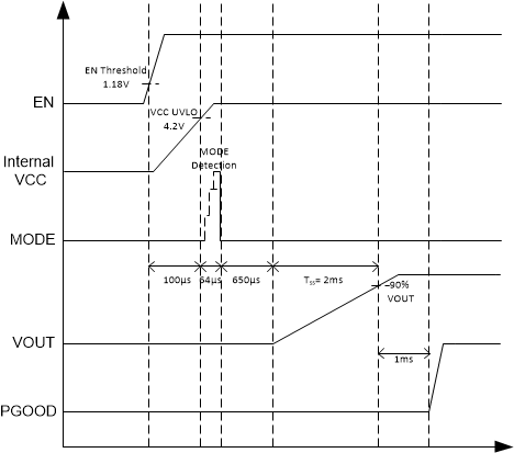
Figure 15 below shows the typical start-up sequence of the device once the enable signal triggers the EN turn-on threshold. After the voltage of internal VCC crosses the UVLO rising threshold, it takes about 64µs to finish the reading and setting of MODE. After this process, the MODE is latched and will not change until VIN or EN toggles to restart-up this device. Then after a delay of around 650µs the internal soft-start function begins to ramp up the reference voltage to the PWM comparator.
Table 1. MODE Pin Settings
| MODE Pin | Light Load Operation Mode | |||
|---|---|---|---|---|
| Short to GND (≤10kΩ) | Eco-mode™ | |||
| Floating (≥500kΩ) | FCCM | |||
 Figure 15. Power-Up Sequence