SWCS138E June 2017 – December 2022 TPS650864
PRODUCTION DATA
- 1 Features
- 2 Applications
- 3 Description
- 4 Revision History
- 5 Device Comparison Table
- 6 Pin Configuration and Functions
-
7 Specifications
- 7.1 Absolute Maximum Ratings
- 7.2 ESD Ratings
- 7.3 Recommended Operating Conditions
- 7.4 Thermal Information
- 7.5 Electrical Characteristics: Total Current Consumption
- 7.6 Electrical Characteristics: Reference and Monitoring System
- 7.7 Electrical Characteristics: Buck Controllers
- 7.8 Electrical Characteristics: Synchronous Buck Converters
- 7.9 Electrical Characteristics: LDOs
- 7.10 Electrical Characteristics: Load Switches
- 7.11 Digital Signals: I2C Interface
- 7.12 Digital Input Signals (CTLx)
- 7.13 Digital Output Signals (IRQB, GPOx)
- 7.14 Timing Requirements
- 7.15 Switching Characteristics
- 7.16 Typical Characteristics
-
8 Detailed Description
- 8.1 Overview
- 8.2 Functional Block Diagram
- 8.3 TPS6508640 Design and Settings
- 8.4 TPS65086401 Design and Settings
- 8.5 TPS6508641 Design and Settings
- 8.6 TPS65086470 Design and Settings
- 8.7 SMPS Voltage Regulators
- 8.8 LDOs and Load Switches
- 8.9 Power Goods (PGOOD or PG) and GPOs
- 8.10 Power Sequencing and VR Control
- 8.11 Device Functional Modes
- 8.12 I2C Interface
- 8.13
Register Maps
- 8.13.1 Register Map Summary
- 8.13.2 DEVICEID1: 1st PMIC Device and Revision ID Register (offset = 00h) [reset = X]
- 8.13.3 DEVICEID2: 2nd PMIC Device and Revision ID Register (offset = 01h) [reset = X]
- 8.13.4 IRQ: PMIC Interrupt Register (offset = 02h) [reset = 0000 0000]
- 8.13.5 IRQ_MASK: PMIC Interrupt Mask Register (offset = 03h) [reset = 1111 1111]
- 8.13.6 PMICSTAT: PMIC Status Register (offset = 04h) [reset = 0000 0000]
- 8.13.7 SHUTDNSRC: PMIC Shut-Down Event Register (offset = 05h) [reset = 0000 0000]
- 8.13.8 BUCK1CTRL: BUCK1 Control Register (offset = 20h) [reset = X]
- 8.13.9 BUCK2CTRL: BUCK2 Control Register (offset = 21h) [reset = X]
- 8.13.10 BUCK3DECAY: BUCK3 Decay Control Register (offset = 22h) [reset = X]
- 8.13.11 BUCK3VID: BUCK3 VID Register (offset = 23h) [reset = X]
- 8.13.12 BUCK3SLPCTRL: BUCK3 Sleep Control VID Register (offset = 24h) [reset = X]
- 8.13.13 BUCK4CTRL: BUCK4 Control Register (offset = 25h) [reset = X]
- 8.13.14 BUCK5CTRL: BUCK5 Control Register (offset = 26h) [reset = X]
- 8.13.15 BUCK6CTRL: BUCK6 Control Register (offset = 27h) [reset = X]
- 8.13.16 LDOA2CTRL: LDOA2 Control Register (offset = 28h) [reset = X]
- 8.13.17 LDOA3CTRL: LDOA3 Control Register (offset = 29h) [reset = X]
- 8.13.18 DISCHCTRL1: 1st Discharge Control Register (offset = 40h) [reset = X]
- 8.13.19 DISCHCTRL2: 2nd Discharge Control Register (offset = 41h) [reset = X]
- 8.13.20 DISCHCTRL3: 3rd Discharge Control Register (offset = 42h) [reset = X]
- 8.13.21 PG_DELAY1: 1st Power Good Delay Register (offset = 43h) [reset = X]
- 8.13.22 FORCESHUTDN: Force Emergency Shutdown Control Register (offset = 91h) [reset = 0000 0000]
- 8.13.23 BUCK1SLPCTRL: BUCK1 Sleep Control Register (offset = 92h) [reset = X]
- 8.13.24 BUCK2SLPCTRL: BUCK2 Sleep Control Register (offset = 93h) [reset = X]
- 8.13.25 BUCK4VID: BUCK4 VID Register (offset = 94h) [reset = X]
- 8.13.26 BUCK4SLPVID: BUCK4 Sleep VID Register (offset = 95h) [reset = X]
- 8.13.27 BUCK5VID: BUCK5 VID Register (offset = 96h) [reset = X]
- 8.13.28 BUCK5SLPVID: BUCK5 Sleep VID Register (offset = 97h) [reset = X]
- 8.13.29 BUCK6VID: BUCK6 VID Register (offset = 98h) [reset = X]
- 8.13.30 BUCK6SLPVID: BUCK6 Sleep VID Register (offset = 99h) [reset = X]
- 8.13.31 LDOA2VID: LDOA2 VID Register (offset = 9Ah) [reset = X]
- 8.13.32 LDOA3VID: LDOA3 VID Register (offset = 9Bh) [reset = X]
- 8.13.33 BUCK123CTRL: BUCK1-3 Control Register (offset = 9Ch) [reset = X]
- 8.13.34 PG_DELAY2: 2nd Power Good Delay Register (offset = 9Dh) [reset = X]
- 8.13.35 SWVTT_DIS: SWVTT Disable Register (offset = 9Fh) [reset = X]
- 8.13.36 I2C_RAIL_EN1: 1st VR Pin Enable Override Register (offset = A0h) [reset = X]
- 8.13.37 I2C_RAIL_EN2/GPOCTRL: 2nd VR Pin Enable Override and GPO Control Register (offset = A1h) [reset = X]
- 8.13.38 PWR_FAULT_MASK1: 1st VR Power Fault Mask Register (offset = A2h) [reset = X]
- 8.13.39 PWR_FAULT_MASK2: 2nd VR Power Fault Mask Register (offset = A3h) [reset = X]
- 8.13.40 GPO1PG_CTRL1: 1st GPO1 PG Control Register (offset = A4h) [reset = X]
- 8.13.41 GPO1PG_CTRL2: 2nd GPO1 PG Control Register (offset = A5h) [reset = X]
- 8.13.42 GPO4PG_CTRL1: 1st GPO4 PG Control Register (offset = A6h) [reset = X]
- 8.13.43 GPO4PG_CTRL2: 2nd GPO4 PG Control Register (offset = A7h) [reset = X]
- 8.13.44 GPO2PG_CTRL1: 1st GPO2 PG Control Register (offset = A8h) [reset = X]
- 8.13.45 GPO2PG_CTRL2: 2nd GPO2 PG Control Register (offset = A9h) [reset = X]
- 8.13.46 GPO3PG_CTRL1: 1st GPO3 PG Control Register (offset = AAh) [reset = X]
- 8.13.47 GPO3PG_CTRL2: 2nd GPO3 PG Control Register (offset = ABh) [reset = X]
- 8.13.48 MISCSYSPG Register (offset = ACh) [reset = X]
- 8.13.49 LDOA1_SWB2_CTRL: LDOA1 and SWB2 Control Register (offset = AEh) [reset = X]
- 8.13.50 PG_STATUS1: 1st Power Good Status Register (offset = B0h) [reset = 0000 0000]
- 8.13.51 PG_STATUS2: 2nd Power Good Status Register (offset = B1h) [reset = 0000 0000]
- 8.13.52 PWR_FAULT_STATUS1: 1st Power Fault Status Register (offset = B2h) [reset = 0000 0000]
- 8.13.53 PWR_FAULT_STATUS2: 2nd Power Fault Status Register (offset = B3h) [reset = 0000 0000]
- 8.13.54 TEMPCRIT: Temperature Fault Status Register (offset = B4h) [reset = 0000 0000]
- 8.13.55 TEMPHOT: Temperature Hot Status Register (offset = B5h) [reset = 0000 0000]
- 8.13.56 OC_STATUS: Overcurrent Fault Status Register (offset = B6h) [reset = 0000 0000]
-
9 Applications, Implementation, and Layout
- 9.1 Application Information
- 9.2 Typical Application
- 9.3 Power Supply Coupling and Bulk Capacitors
- 9.4 Do's and Don'ts
- 10Device and Documentation Support
- 11Mechanical, Packaging, and Orderable Information
Package Options
Mechanical Data (Package|Pins)
- RSK|64
Thermal pad, mechanical data (Package|Pins)
- RSK|64
Orderable Information
8.7.5 Current Limit
The buck controllers (BUCK1, BUCK2, and BUCK6) have inductor-valley current-limit architecture and the current limit is programmable by an external resistor at the ILIMx pin. Equation 1 shows the calculation for a desired resistor value, depending on specific application conditions. ILIMREF is the current source out of the ILIMx pin that is typically 50 µA, and RDSON is the maximum channel resistance of the low-side FET. The scaling factor is 1.3 to take into account all errors and temperature variations of RDSON, ILIMREF, and RILIM. Finally, 8 is another scaling factor associated with ILIMREF.
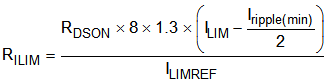
where
- ILIM is the target current limit. An appropriate margin must be allowed when determining ILIM from maximum output DC load current.
- Iripple(min) is the minimum peak-to-peak inductor ripple current for a given VOUT.
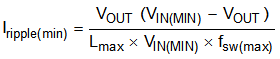
where
- Lmax is maximum inductance
- fsw(max) is maximum switching frequency
- VIN(MIN) minimum input voltage to the external power stage
The buck converter limit inductor peak current cycle-by-cycle to IIND_LIM is specified in Section 7.8.
The current limit circuit also protects against reverse current going back into the low side FET from the load. When operating in Force PWM mode, the inductor current is expected to go negative so it is important to ensure that the RILIM value is sufficient to account for this. If operating in PFM, this can be neglected. The equation for Force PWM minimum RILIM value is:
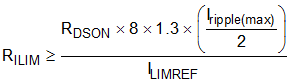
where
- Iripple(max) is the maximum peak-to-peak inductor ripple current for a given VOUT.
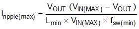
where
- Lmin is minimum inductance
- fsw(min) is minimum switching frequency
- VIN(MAX) maximum input voltage to the external power stage
If RILIM is too low for the chosen inductor and voltage conditions, then the ripple current at no load will trigger the negative current limit, forcing the low side FET to turn off. This will eventually result in the output voltage increasing above target regulation point due to irregular duty cycle created by current limit being triggered.