SWCS138E June 2017 – December 2022 TPS650864
PRODUCTION DATA
- 1 Features
- 2 Applications
- 3 Description
- 4 Revision History
- 5 Device Comparison Table
- 6 Pin Configuration and Functions
-
7 Specifications
- 7.1 Absolute Maximum Ratings
- 7.2 ESD Ratings
- 7.3 Recommended Operating Conditions
- 7.4 Thermal Information
- 7.5 Electrical Characteristics: Total Current Consumption
- 7.6 Electrical Characteristics: Reference and Monitoring System
- 7.7 Electrical Characteristics: Buck Controllers
- 7.8 Electrical Characteristics: Synchronous Buck Converters
- 7.9 Electrical Characteristics: LDOs
- 7.10 Electrical Characteristics: Load Switches
- 7.11 Digital Signals: I2C Interface
- 7.12 Digital Input Signals (CTLx)
- 7.13 Digital Output Signals (IRQB, GPOx)
- 7.14 Timing Requirements
- 7.15 Switching Characteristics
- 7.16 Typical Characteristics
-
8 Detailed Description
- 8.1 Overview
- 8.2 Functional Block Diagram
- 8.3 TPS6508640 Design and Settings
- 8.4 TPS65086401 Design and Settings
- 8.5 TPS6508641 Design and Settings
- 8.6 TPS65086470 Design and Settings
- 8.7 SMPS Voltage Regulators
- 8.8 LDOs and Load Switches
- 8.9 Power Goods (PGOOD or PG) and GPOs
- 8.10 Power Sequencing and VR Control
- 8.11 Device Functional Modes
- 8.12 I2C Interface
- 8.13
Register Maps
- 8.13.1 Register Map Summary
- 8.13.2 DEVICEID1: 1st PMIC Device and Revision ID Register (offset = 00h) [reset = X]
- 8.13.3 DEVICEID2: 2nd PMIC Device and Revision ID Register (offset = 01h) [reset = X]
- 8.13.4 IRQ: PMIC Interrupt Register (offset = 02h) [reset = 0000 0000]
- 8.13.5 IRQ_MASK: PMIC Interrupt Mask Register (offset = 03h) [reset = 1111 1111]
- 8.13.6 PMICSTAT: PMIC Status Register (offset = 04h) [reset = 0000 0000]
- 8.13.7 SHUTDNSRC: PMIC Shut-Down Event Register (offset = 05h) [reset = 0000 0000]
- 8.13.8 BUCK1CTRL: BUCK1 Control Register (offset = 20h) [reset = X]
- 8.13.9 BUCK2CTRL: BUCK2 Control Register (offset = 21h) [reset = X]
- 8.13.10 BUCK3DECAY: BUCK3 Decay Control Register (offset = 22h) [reset = X]
- 8.13.11 BUCK3VID: BUCK3 VID Register (offset = 23h) [reset = X]
- 8.13.12 BUCK3SLPCTRL: BUCK3 Sleep Control VID Register (offset = 24h) [reset = X]
- 8.13.13 BUCK4CTRL: BUCK4 Control Register (offset = 25h) [reset = X]
- 8.13.14 BUCK5CTRL: BUCK5 Control Register (offset = 26h) [reset = X]
- 8.13.15 BUCK6CTRL: BUCK6 Control Register (offset = 27h) [reset = X]
- 8.13.16 LDOA2CTRL: LDOA2 Control Register (offset = 28h) [reset = X]
- 8.13.17 LDOA3CTRL: LDOA3 Control Register (offset = 29h) [reset = X]
- 8.13.18 DISCHCTRL1: 1st Discharge Control Register (offset = 40h) [reset = X]
- 8.13.19 DISCHCTRL2: 2nd Discharge Control Register (offset = 41h) [reset = X]
- 8.13.20 DISCHCTRL3: 3rd Discharge Control Register (offset = 42h) [reset = X]
- 8.13.21 PG_DELAY1: 1st Power Good Delay Register (offset = 43h) [reset = X]
- 8.13.22 FORCESHUTDN: Force Emergency Shutdown Control Register (offset = 91h) [reset = 0000 0000]
- 8.13.23 BUCK1SLPCTRL: BUCK1 Sleep Control Register (offset = 92h) [reset = X]
- 8.13.24 BUCK2SLPCTRL: BUCK2 Sleep Control Register (offset = 93h) [reset = X]
- 8.13.25 BUCK4VID: BUCK4 VID Register (offset = 94h) [reset = X]
- 8.13.26 BUCK4SLPVID: BUCK4 Sleep VID Register (offset = 95h) [reset = X]
- 8.13.27 BUCK5VID: BUCK5 VID Register (offset = 96h) [reset = X]
- 8.13.28 BUCK5SLPVID: BUCK5 Sleep VID Register (offset = 97h) [reset = X]
- 8.13.29 BUCK6VID: BUCK6 VID Register (offset = 98h) [reset = X]
- 8.13.30 BUCK6SLPVID: BUCK6 Sleep VID Register (offset = 99h) [reset = X]
- 8.13.31 LDOA2VID: LDOA2 VID Register (offset = 9Ah) [reset = X]
- 8.13.32 LDOA3VID: LDOA3 VID Register (offset = 9Bh) [reset = X]
- 8.13.33 BUCK123CTRL: BUCK1-3 Control Register (offset = 9Ch) [reset = X]
- 8.13.34 PG_DELAY2: 2nd Power Good Delay Register (offset = 9Dh) [reset = X]
- 8.13.35 SWVTT_DIS: SWVTT Disable Register (offset = 9Fh) [reset = X]
- 8.13.36 I2C_RAIL_EN1: 1st VR Pin Enable Override Register (offset = A0h) [reset = X]
- 8.13.37 I2C_RAIL_EN2/GPOCTRL: 2nd VR Pin Enable Override and GPO Control Register (offset = A1h) [reset = X]
- 8.13.38 PWR_FAULT_MASK1: 1st VR Power Fault Mask Register (offset = A2h) [reset = X]
- 8.13.39 PWR_FAULT_MASK2: 2nd VR Power Fault Mask Register (offset = A3h) [reset = X]
- 8.13.40 GPO1PG_CTRL1: 1st GPO1 PG Control Register (offset = A4h) [reset = X]
- 8.13.41 GPO1PG_CTRL2: 2nd GPO1 PG Control Register (offset = A5h) [reset = X]
- 8.13.42 GPO4PG_CTRL1: 1st GPO4 PG Control Register (offset = A6h) [reset = X]
- 8.13.43 GPO4PG_CTRL2: 2nd GPO4 PG Control Register (offset = A7h) [reset = X]
- 8.13.44 GPO2PG_CTRL1: 1st GPO2 PG Control Register (offset = A8h) [reset = X]
- 8.13.45 GPO2PG_CTRL2: 2nd GPO2 PG Control Register (offset = A9h) [reset = X]
- 8.13.46 GPO3PG_CTRL1: 1st GPO3 PG Control Register (offset = AAh) [reset = X]
- 8.13.47 GPO3PG_CTRL2: 2nd GPO3 PG Control Register (offset = ABh) [reset = X]
- 8.13.48 MISCSYSPG Register (offset = ACh) [reset = X]
- 8.13.49 LDOA1_SWB2_CTRL: LDOA1 and SWB2 Control Register (offset = AEh) [reset = X]
- 8.13.50 PG_STATUS1: 1st Power Good Status Register (offset = B0h) [reset = 0000 0000]
- 8.13.51 PG_STATUS2: 2nd Power Good Status Register (offset = B1h) [reset = 0000 0000]
- 8.13.52 PWR_FAULT_STATUS1: 1st Power Fault Status Register (offset = B2h) [reset = 0000 0000]
- 8.13.53 PWR_FAULT_STATUS2: 2nd Power Fault Status Register (offset = B3h) [reset = 0000 0000]
- 8.13.54 TEMPCRIT: Temperature Fault Status Register (offset = B4h) [reset = 0000 0000]
- 8.13.55 TEMPHOT: Temperature Hot Status Register (offset = B5h) [reset = 0000 0000]
- 8.13.56 OC_STATUS: Overcurrent Fault Status Register (offset = B6h) [reset = 0000 0000]
-
9 Applications, Implementation, and Layout
- 9.1 Application Information
- 9.2 Typical Application
- 9.3 Power Supply Coupling and Bulk Capacitors
- 9.4 Do's and Don'ts
- 10Device and Documentation Support
- 11Mechanical, Packaging, and Orderable Information
Package Options
Mechanical Data (Package|Pins)
- RSK|64
Thermal pad, mechanical data (Package|Pins)
- RSK|64
Orderable Information
8.12.1 F/S-Mode Protocol
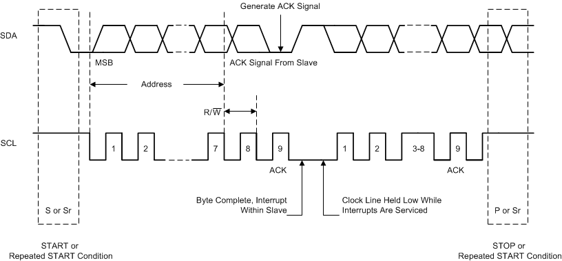
The master initiates data transfer by generating a start condition. The start condition is when a high-to-low transition occurs on the SDA line while SCL is high (see Figure 8-28). All I2C-compatible devices should recognize a start condition.
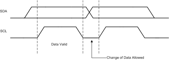
The master then generates the SCL pulses, and transmits the 7-bit address and the read/write direction bit R/W on the SDA line. During all transmissions, the master ensures that data is valid. A valid data condition requires the SDA line to be stable during the entire high period of the clock pulse (see
Figure 8-29). All devices recognize the address sent by the master and compare it to their internal fixed addresses. Only the slave device with a matching address generates an acknowledge (see Figure 8-30), by pulling the SDA line low during the entire high period of the ninth SCL cycle. Upon detecting this acknowledge, the master knows that the communication link with a slave has been established.
The master generates further SCL cycles to either transmit data to the slave (R/W bit = 0) or receive data from the slave (R/W bit = 1). In either case, the receiver needs to acknowledge the data sent by the transmitter. An acknowledge signal can either be generated by the master or by the slave, depending on which one is the receiver. 9-bit valid data sequences consisting of 8-bit data and 1-bit acknowledge can continue as long as necessary.
To signal the end of the data transfer, the master generates a stop condition by pulling the SDA line from low to high while the SCL line is high (see Figure 8-28). This releases the bus and stops the communication link with the addressed slave. All I2C-compatible devices must recognize the stop condition. Upon the receipt of a stop condition, all devices know that the bus is released, and they wait for a start condition followed by a matching address.
 Figure 8-28 START and STOP Conditions
 Figure 8-29 Bit Transfer on the I2C Bus
 Figure 8-30 Acknowledge on the I2C Bus
 Figure 8-31 I2C Bus Protocol
 Figure 8-32 I2C Interface WRITE to TPS650864 in F/S Mode
 Figure 8-33 I2C Interface READ from TPS650864 in F/S Mode (Only Repeated START is Supported)