SLVSCJ5B December 2015 – June 2020 TPS7H3301-SP
PRODUCTION DATA.
- 1 Features
- 2 Applications
- 3 Description
- 4 Revision History
- 5 Pin Configuration and Functions
- 6 Specifications
- 7 Detailed Description
-
8 Application and Implementation
- 8.1 Application Information
- 8.2
Typical Application
- 8.2.1 Design Requirements
- 8.2.2
Detailed Design Procedure
- 8.2.2.1 VDD/VIN Capacitor
- 8.2.2.2 VLDO Input Capacitor
- 8.2.2.3 VTT Output Capacitor
- 8.2.2.4 VTTSNS Connection
- 8.2.2.5 Low VIN Applications
- 8.2.2.6 S3 and Pseudo-S5 Support
- 8.2.2.7 Tracking Startup and Shutdown
- 8.2.2.8 Output Tolerance Consideration for VTT DIMM or Module Applications
- 8.2.2.9 LDO Design Guidelines
- 8.2.3 Application Curve
- 9 Power Supply Recommendations
- 10Layout
- 11Device and Documentation Support
- 12Mechanical, Packaging, and Orderable Information
Package Options
Mechanical Data (Package|Pins)
- HKR|16
Thermal pad, mechanical data (Package|Pins)
Orderable Information
3 Description
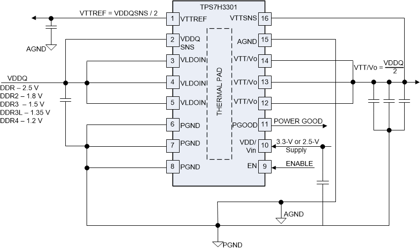
The TPS7H3301-SP is a TID and SEE radiation-hardened double data rate (DDR) 3-A termination regulator with built-in VTTREF buffer. The regulator is specifically designed to provide a complete, compact, low-noise solution for space DDR termination applications such as single board computers, solid state recorders, and payload processing.
The TPS7H3301-SP supports DDR VTT termination applications using DDR, DDR2, DDR3, DDR4. The fast transient response of the TPS7H3301-SP VTT regulator allows for a very stable supply during read/write conditions. During transients, the fast tracking feature of the VTTREF supply minimizes any voltage offset between VTT/Vo and VTTREF. To enable simple power sequencing, both an enable input and a power-good output (PGOOD) have been integrated into the TPS7H3301-SP. The PGOOD output is open-drain so it can be tied to multiple open-drain outputs to monitor when all supplies have come into regulation. The enable signal can also be used to discharge VTT/Vo during suspend to RAM (S3) power down mode.
Device Information(1)
| PART NUMBER | GRADE | PACKAGE |
|---|---|---|
| 5962R1422801VXC | Flight Grade RHA 100 krad(Si) | 16-Pin CFP
9.60 mm × 11.00 mm Weight: 1.55 g(5) |
| 5962-1422801VXC | Flight Grade QMLV | |
| TPS7H3301HKR/EM | Engineering Module(4) | |
| TPS7H3301EVM-CVAL | Ceramic Evaluation Board | EVM |
- For all available packages, see the orderable addendum at the end of the data sheet.
- See Radiation Report for details.
- Applicable to DDR2, DDR3, DDR3L and DDR4. For DDR, input voltage = 3.3-V nominal. VIN is 2.95 to 3.5 V for DDR1 and VLDOIN > VTT/VO for all DDRs.
For DDR2 3-A load condition, VIN is 2.45 to 3.5 V.
VIN headroom: VIN_MIN ≥ VTT/VO + 1.5 V. - These units are intended for engineering evaluation only. They are processed to a noncompliant flow (that is, no burn-in, and so forth) and are tested to a temperature rating of 25°C only. These units are not suitable for qualification, production, radiation testing or flight use. Parts are not warranted for performance over the full MIL specified temperature range of –55°C to 125°C or operating life.
- Weight is accurate to ±10%.
