SLVSCJ5B December 2015 – June 2020 TPS7H3301-SP
PRODUCTION DATA.
- 1 Features
- 2 Applications
- 3 Description
- 4 Revision History
- 5 Pin Configuration and Functions
- 6 Specifications
- 7 Detailed Description
-
8 Application and Implementation
- 8.1 Application Information
- 8.2
Typical Application
- 8.2.1 Design Requirements
- 8.2.2
Detailed Design Procedure
- 8.2.2.1 VDD/VIN Capacitor
- 8.2.2.2 VLDO Input Capacitor
- 8.2.2.3 VTT Output Capacitor
- 8.2.2.4 VTTSNS Connection
- 8.2.2.5 Low VIN Applications
- 8.2.2.6 S3 and Pseudo-S5 Support
- 8.2.2.7 Tracking Startup and Shutdown
- 8.2.2.8 Output Tolerance Consideration for VTT DIMM or Module Applications
- 8.2.2.9 LDO Design Guidelines
- 8.2.3 Application Curve
- 9 Power Supply Recommendations
- 10Layout
- 11Device and Documentation Support
- 12Mechanical, Packaging, and Orderable Information
Package Options
Mechanical Data (Package|Pins)
- HKR|16
Thermal pad, mechanical data (Package|Pins)
Orderable Information
8.2.2.9 LDO Design Guidelines
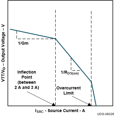
The minimum input (VLDOIN) to output voltage (VTT/VO) difference (headroom) decides the lowest usable supply voltage Gm-driven to drive a certain load. For TPS7H3301-SP, a minimum of 300 mV (VLDOINMIN – VTT/VOMAX) is needed in order to support a Gm driven sourcing current of 3 A based on a design of VLDOIN = 3.3 V and COUT = 470 μF. Because the TPS7H3301-SP is essentially a Gm-driven LDO, its impedance characteristics are both a function of the 1/Gm and RDS(on) of the sourcing MOSFET (see Figure 22). The current inflection point of the design is between 3 A and 4 A. When ISRC is less than the inflection point, the LDO is considered to be operating in the Gm region; when ISRC is greater than the inflection point but less than the overcurrent limit point, the LDO is operating in the RDS(on) region. The typical sourcing RDS(on) is 154 mΩ with V IN = 3 V and TJ = 125°C.
 Figure 22. TPS7H3301-SP Impedance Characteristics