SLUSAW0B March 2012 – December 2023 UCC28070A
PRODUCTION DATA
- 1
- 1 Features
- 2 Applications
- 3 Description
- 4 Pin Configuration and Functions
- 5 Specifications
-
6 Detailed Description
- 6.1 Overview
- 6.2 Functional Block Diagram
- 6.3
Feature Description
- 6.3.1 Interleaving
- 6.3.2 Programming the PWM Frequency and Maximum Duty-Cycle Clamp
- 6.3.3 Frequency Dithering (Magnitude and Rate)
- 6.3.4 External Clock Synchronization
- 6.3.5 Multi-phase Operation
- 6.3.6 VSENSE and VINAC Resistor Configuration
- 6.3.7 VSENSE and VINAC Open-Circuit Protection
- 6.3.8 Current Synthesizer
- 6.3.9 Programmable Peak Current Limit
- 6.3.10 Linear Multiplier and Quantized Voltage Feed Forward
- 6.3.11 Enhanced Transient Response (VA Slew-Rate Correction)
- 6.3.12 Voltage Biasing (VCC and VVREF)
- 6.3.13 PFC Enable and Disable
- 6.3.14 Adaptive Soft Start
- 6.3.15 PFC Start-Up Hold Off
- 6.3.16 Output Overvoltage Protection (OVP)
- 6.3.17 Zero-Power Detection
- 6.3.18 Thermal Shutdown
- 6.3.19 Current Loop Compensation
- 6.3.20 Voltage Loop Compensation
- 6.4 Device Functional Modes
-
7 Application and Implementation
- 7.1 Application Information
- 7.2
Typical Application
- 7.2.1 Design Requirements
- 7.2.2
Detailed Design Procedure
- 7.2.2.1 Output Current Calculation
- 7.2.2.2 Bridge Rectifier
- 7.2.2.3 PFC Inductor (L1 and L2)
- 7.2.2.4 PFC MOSFETs (M1 and M2)
- 7.2.2.5 PFC Diode
- 7.2.2.6 PFC Output Capacitor
- 7.2.2.7 Current-Loop Feedback Configuration (Sizing of the Current-Transformer Turns-Ratio and Sense Resistor (RS))
- 7.2.2.8 Current-Sense Offset and PWM Ramp for Improved Noise Immunity
- 7.2.3 Application Curves
- 7.3 Power Supply Recommendations
- 7.4 Layout
- 8 Device and Documentation Support
- 9 Revision History
- 10Mechanical, Packaging, and Orderable Information
Package Options
Mechanical Data (Package|Pins)
- PW|20
Thermal pad, mechanical data (Package|Pins)
- PW|20
Orderable Information
6.3.19 Current Loop Compensation
The UCC28070A incorporates two identical and independent transconductance-type current-error amplifiers (one for each phase) with which to control the shaping of the PFC input current waveform. The current-error amplifier (CA) forms the heart of the embedded current control loop of the boost PFC preregulator, and is compensated for loop stability using familiar principles [7, 8]. The output of the CA for phase-A is CAOA, and that for phase-B is CAOB. Because the design considerations are the same for both, they are collectively referred to as CAOx, where x is A or B.
In a boost PFC preregulator, the current control loop comprises the boost power plant stage, the current sensing circuitry, the wave-shape reference, the PWM stage, and the CA with compensation components. The CA compares the average boost inductor current sensed with the wave-shape reference from the multiplier stage and generates an output current proportional to the difference.
This CA output current flows through the impedance of the compensation network generating an output voltage, VCAO, which is then compared with a periodic voltage ramp to generate the PWM signal necessary to achieve PFC.
 Figure 6-5 Current
Error Amplifier With Type II Compensation
Figure 6-5 Current
Error Amplifier With Type II CompensationFor frequencies above boost LC resonance and below fPWM, the small-signal model of the boost stage, which includes current sensing, can be simplified to:
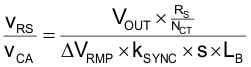
where:
- LB = mid-value boost inductance
- RS = CT sense resistor
- NCT = CT turns ratio
- VOUT = average output voltage of the PFC converter
- ∆VRMP = 4Vpk-pk amplitude of the PWM voltage ramp
- kSYNC = ramp reduction factor due to external synchronization frequency: kSYNC = (15000 / RRT(kΩ)) / fSYNC, where RRT(kΩ) is from Equation 8. When external synchronization is not used, kSYNC = 1.
- s = Laplace complex variable
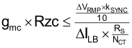
An RZC-CZC network is introduced on CAOx to obtain high gain for the low-frequency content of the inductor current signal, but reduced flat gain above the zero frequency out to fPWM to attenuate the high-frequency switching ripple content of the signal (thus averaging it).
The switching ripple voltage must be attenuated to less than 1/10 of the ΔVRMP amplitude so as to be considered negligible ripple.
Thus, CAOx gain at fPWM is:
where:
- ∆ILB is the maximum peak-to-peak ripple current in the boost inductor
- gmc is the transconductance of the CA, 100μS
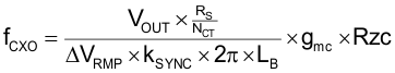
The current-loop cross-over frequency is then found by equating the open loop gain to 1 and solving for fCXO:
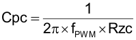
CZC is then determined by setting fZC = fCXO = 1 / (2π × RZC × CZC) and solving for CZC. At fZC = fCXO, a phase margin of 45° is obtained at fCXO. Greater phase margin may be had by placing fZC < fCXO.
An additional high-frequency pole is generally added at fPWM to further attenuate ripple and noise at fPWM and higher. This is done by adding a small-value capacitor, CPC, across the RZCCZCnetwork.
The procedure above is valid for fixed-value inductors.
If a "swinging-choke" boost inductor (inductance decreases gradually with increasing current) is used, fCXO varies with inductance, so CZC must be determined at maximum inductance.