SLUSAW0B March 2012 – December 2023 UCC28070A
PRODUCTION DATA
- 1
- 1 Features
- 2 Applications
- 3 Description
- 4 Pin Configuration and Functions
- 5 Specifications
-
6 Detailed Description
- 6.1 Overview
- 6.2 Functional Block Diagram
- 6.3
Feature Description
- 6.3.1 Interleaving
- 6.3.2 Programming the PWM Frequency and Maximum Duty-Cycle Clamp
- 6.3.3 Frequency Dithering (Magnitude and Rate)
- 6.3.4 External Clock Synchronization
- 6.3.5 Multi-phase Operation
- 6.3.6 VSENSE and VINAC Resistor Configuration
- 6.3.7 VSENSE and VINAC Open-Circuit Protection
- 6.3.8 Current Synthesizer
- 6.3.9 Programmable Peak Current Limit
- 6.3.10 Linear Multiplier and Quantized Voltage Feed Forward
- 6.3.11 Enhanced Transient Response (VA Slew-Rate Correction)
- 6.3.12 Voltage Biasing (VCC and VVREF)
- 6.3.13 PFC Enable and Disable
- 6.3.14 Adaptive Soft Start
- 6.3.15 PFC Start-Up Hold Off
- 6.3.16 Output Overvoltage Protection (OVP)
- 6.3.17 Zero-Power Detection
- 6.3.18 Thermal Shutdown
- 6.3.19 Current Loop Compensation
- 6.3.20 Voltage Loop Compensation
- 6.4 Device Functional Modes
-
7 Application and Implementation
- 7.1 Application Information
- 7.2
Typical Application
- 7.2.1 Design Requirements
- 7.2.2
Detailed Design Procedure
- 7.2.2.1 Output Current Calculation
- 7.2.2.2 Bridge Rectifier
- 7.2.2.3 PFC Inductor (L1 and L2)
- 7.2.2.4 PFC MOSFETs (M1 and M2)
- 7.2.2.5 PFC Diode
- 7.2.2.6 PFC Output Capacitor
- 7.2.2.7 Current-Loop Feedback Configuration (Sizing of the Current-Transformer Turns-Ratio and Sense Resistor (RS))
- 7.2.2.8 Current-Sense Offset and PWM Ramp for Improved Noise Immunity
- 7.2.3 Application Curves
- 7.3 Power Supply Recommendations
- 7.4 Layout
- 8 Device and Documentation Support
- 9 Revision History
- 10Mechanical, Packaging, and Orderable Information
Package Options
Mechanical Data (Package|Pins)
- PW|20
Thermal pad, mechanical data (Package|Pins)
- PW|20
Orderable Information
6.3.1 Interleaving
One of the main benefits from the 180° interleaving of phases is significant reductions in the high-frequency ripple components of both the input current and the current into the output capacitor of the PFC preregulator. Compared to that of a single-phase PFC stage of equal power, the reduced ripple on the input current eases the burden of filtering conducted-EMI noise and helps reduce the EMI filter and CIN sizes. Additionally, reduced high-frequency ripple current into the PFC output capacitor, COUT, helps to reduce its size and cost. Furthermore, with reduced ripple and average current in each phase, the boost inductor size can be smaller than in a single-phase design [3].
Ripple current reduction due to interleaving is often referred to as ripple cancellation, but strictly speaking, the peak-to-peak ripple is completely cancelled only at 50% duty-cycle in a 2-phase system. At duty-cycles other than 50%, ripple reduction occurs in the form of partial cancellation due to the superposition of the individual phase currents. Nevertheless, compared to the ripple currents of an equivalent single-phase PFC preregulator, those of a 2-phase interleaved design are extraordinarily smaller [3]. Independent of ripple cancellation, the frequency of the interleaved ripple, at both the input and output, is 2 × fPWM.
At the PFC input, 180° interleaving reduces the peak-to-peak current-ripple amplitude to ½ or less of the ripple amplitude of the equivalent single-phase current.
At the PFC output, 180° interleaving reduces the rms value of the PFC-generated ripple current in the output capacitor by a factor of slightly more than √ 2, for PWM duty-cycles > 50%.
This can be seen in the following derivations, adapting the method by Erickson [4].
In a single-phase PFC preregulator, the total rms capacitor current contributed by the PFC stage at all duty-cycles can be shown to be approximated by:
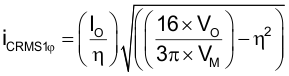
where
- IO is the average PFC output load current
- VO is the average PFC output voltage
- VM is the peak of the input AC-line voltage
- η is the efficiency of the PFC stage at these conditions
In a dual-phase interleaved PFC preregulator, the total rms capacitor current contributed by the PFC stage for D > 50% can be shown to be approximated by:

It can be seen that the quantity under the radical for iCRMS2φ is slightly smaller than ½ of that under the radical for iCRMS1φ. The rms currents shown contain both the low-frequency and the high-frequency components of the PFC output current. Interleaving reduces the high-frequency component, but not the low-frequency component.