SLUSAW0B March 2012 – December 2023 UCC28070A
PRODUCTION DATA
- 1
- 1 Features
- 2 Applications
- 3 Description
- 4 Pin Configuration and Functions
- 5 Specifications
-
6 Detailed Description
- 6.1 Overview
- 6.2 Functional Block Diagram
- 6.3
Feature Description
- 6.3.1 Interleaving
- 6.3.2 Programming the PWM Frequency and Maximum Duty-Cycle Clamp
- 6.3.3 Frequency Dithering (Magnitude and Rate)
- 6.3.4 External Clock Synchronization
- 6.3.5 Multi-phase Operation
- 6.3.6 VSENSE and VINAC Resistor Configuration
- 6.3.7 VSENSE and VINAC Open-Circuit Protection
- 6.3.8 Current Synthesizer
- 6.3.9 Programmable Peak Current Limit
- 6.3.10 Linear Multiplier and Quantized Voltage Feed Forward
- 6.3.11 Enhanced Transient Response (VA Slew-Rate Correction)
- 6.3.12 Voltage Biasing (VCC and VVREF)
- 6.3.13 PFC Enable and Disable
- 6.3.14 Adaptive Soft Start
- 6.3.15 PFC Start-Up Hold Off
- 6.3.16 Output Overvoltage Protection (OVP)
- 6.3.17 Zero-Power Detection
- 6.3.18 Thermal Shutdown
- 6.3.19 Current Loop Compensation
- 6.3.20 Voltage Loop Compensation
- 6.4 Device Functional Modes
-
7 Application and Implementation
- 7.1 Application Information
- 7.2
Typical Application
- 7.2.1 Design Requirements
- 7.2.2
Detailed Design Procedure
- 7.2.2.1 Output Current Calculation
- 7.2.2.2 Bridge Rectifier
- 7.2.2.3 PFC Inductor (L1 and L2)
- 7.2.2.4 PFC MOSFETs (M1 and M2)
- 7.2.2.5 PFC Diode
- 7.2.2.6 PFC Output Capacitor
- 7.2.2.7 Current-Loop Feedback Configuration (Sizing of the Current-Transformer Turns-Ratio and Sense Resistor (RS))
- 7.2.2.8 Current-Sense Offset and PWM Ramp for Improved Noise Immunity
- 7.2.3 Application Curves
- 7.3 Power Supply Recommendations
- 7.4 Layout
- 8 Device and Documentation Support
- 9 Revision History
- 10Mechanical, Packaging, and Orderable Information
Package Options
Mechanical Data (Package|Pins)
- PW|20
Thermal pad, mechanical data (Package|Pins)
- PW|20
Orderable Information
6.3.10 Linear Multiplier and Quantized Voltage Feed Forward
The UCC28070A multiplier generates a reference current which represents the desired wave shape and proportional amplitude of the AC input current. This current is converted to a reference voltage signal by the RIMO resistor which is scaled in value to match the voltage of the current-sense signals. The instantaneous multiplier current is dependent upon the rectified, scaled input voltage VVINAC and the voltage-error amplifier output VVAO. VVINAC conveys three pieces of information to the multiplier:
- The overall wave-shape of the input voltage (typically sinusoidal)
- The instantaneous input voltage magnitude at any point in the line cycle
- The rms level of the input voltage.
A major innovation in the UCC28070A multiplier architecture is the internal quantized VRMS feed-forward (QVFF) circuitry, which eliminates the requirement for external filtering of the VINAC signal and the subsequent slow response to transient line variations. A unique circuit algorithm detects the transition of the peak of VVINAC through seven thresholds and generates an equivalent VFF level centered within the 8-QVFF ranges. The boundaries of the ranges expand with increasing VIN to maintain an approximately equal-percentage delta between levels. These 8-QVFF levels are spaced to accommodate the full universal line range of 85VRMS to 265VRMS.
A great benefit of the QVFF architecture is that the fixed kVFF factors eliminate any contribution to distortion of the multiplier output, unlike an externally-filtered VINAC signal which unavoidably contains 2nd-harmonic distortion components. Furthermore, the QVFF algorithm allows for rapid response to both increasing and decreasing changes in input rms voltage so that disturbances transmitted to the PFC output are minimized. 5% hysteresis in the level thresholds help avoid chattering between QVFF levels for VVINAC voltage peaks near a particular threshold or containing mild ringing or distortion. The QVFF architecture requires that the input voltage be largely sinusoidal, and relies on detecting zero-crossings to adjust QVFF downward on decreasing input voltage. Zero-crossings are defined as VVINAC falling below 0.7V for at least 50μs, typically.
Table 6-1 shows the relationship between the various VVINAC peak voltages and the corresponding kVFF terms for the multiplier equation.
| LEVEL | VVINAC PEAK VOLTAGE | kVFF (V2) | VIN PEAK VOLTAGE (1) |
|---|---|---|---|
| 8 | 2.6V ≤ VVINAC(pk) | 3.857 | >345V |
| 7 | 2.25V ≤ VVINAC(pk) < 2.6V | 2.922 | 300V to 345V |
| 6 | 1.95V ≤ VVINAC(pk) < 2.25V | 2.199 | 260V to 300V |
| 5 | 1.65V ≤ VVINAC(pk) < 1.95V | 1.604 | 220V to 260V |
| 4 | 1.4V ≤ VVINAC(pk) < 1.65V | 1.156 | 187V to 220V |
| 3 | 1.2V ≤ VVINAC(pk) < 1.4V | 0.839 | 160V to 187V |
| 2 | 1V ≤ VVINAC(pk) < 1.2V | 0.6 | 133V to 160V |
| 1 | VVINAC(pk) ≤ 1V | 0.398 | <133V |
The multiplier output current IIMO for any line and load condition can thus be determined using Equation 13:
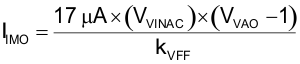
Because the kVFF value represents the scaled (VRMS)2 at the center of a level, VVAO adjusts slightly upwards or downwards when VVINAC(pk) is either lower or higher than the center of the QVFF voltage range to compensate for the difference. This is automatically accomplished by the voltage loop control when VIN varies, both within a level and after a transition between levels.
The output of the voltage-error amplifier (VVAO) is clamped at 5V, which represents the maximum PFC output power. This value is used to calculate the maximum reference current at the IMO pin, and sets a limit for the maximum input power allowed (and, as a consequence, limits maximum output power).
Unlike a continuous VFF situation, where maximum input power is a fixed power at any VRMS input, the discrete QVFF levels permit a variation in maximum input power within limited boundaries as the input VRMS varies within each level.
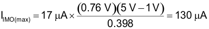
The lowest maximum power limit occurs at the VVINAC voltage of 0.76V, while the highest maximum power limit occurs at the increasing threshold from level-1 to level-2. This pattern repeats at every level transition threshold, considering that decreasing thresholds are 95% of the increasing threshold values. Below VVINAC = 0.76V, PIN is always less than PIN(max), falling linearly to zero with decreasing input voltage.
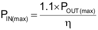
For example, to design for the lowest maximum power allowable, determine the maximum steady-state (average) output power required of the PFC preregulator and add some additional percentage to account for line drop-out recovery power (to recharge COUT while full load power is drawn) such as 10% or 20% of POUT(max). Then apply the expected efficiency factor to find the lowest maximum input power allowable:
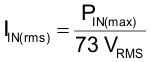
At the PIN(max) design threshold, VVINAC = 0.76V, hence QVFF = 0.398 and input VAC = 73VRMS (accounting for 2V bridge-rectifier drop) for a nominal 400V output system.
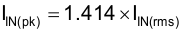
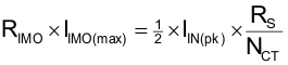
This IIN(pk) value represents the combined average current through the boost inductors at the peak of the line voltage. Each inductor current is detected and scaled by a current-sense transformer (CT). Assuming equal currents through each interleaved phase, the signal voltage at each current sense input pin (CSA and CSB) is developed across a sense resistor selected to generate approximately 3V based on ½ IIN(pk) × RS / NCT, where RS is the current sense resistor and NCT is the CT turns-ratio.
IIMO is then calculated at that same lowest maximum-power point, as:
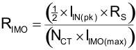
RIMO is selected such that:
Therefore:
At the increasing side of the level-1 to level-2 threshold, note that the IMO current would allow higher input currents at low-line:
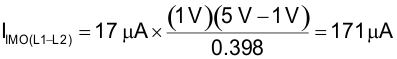
However, this current may easily be limited by the programmable peak current limiting (PKLMT) feature of the UCC28070A if required by the power stage design.
The same procedure can be used to find the lowest and highest input power limits at each of the QVFF level transition thresholds. At higher line voltages, where the average current with inductor ripple is traditionally below the PKLMT threshold, the full variation of maximum input power is seen, but the input currents are inherently below the maximum acceptable current levels of the power stage.
The performance of the multiplier in the UCC28070A has been significantly enhanced when compared to previous generation PFC controllers, with high linearity and accuracy over most of the input ranges. The accuracy is at its worst as VVAO approaches 1V because the error of the (VVAO – 1) subtraction increases and begins to distort the IMO reference current to a greater degree.