SLUSAW0B March 2012 – December 2023 UCC28070A
PRODUCTION DATA
- 1
- 1 Features
- 2 Applications
- 3 Description
- 4 Pin Configuration and Functions
- 5 Specifications
-
6 Detailed Description
- 6.1 Overview
- 6.2 Functional Block Diagram
- 6.3
Feature Description
- 6.3.1 Interleaving
- 6.3.2 Programming the PWM Frequency and Maximum Duty-Cycle Clamp
- 6.3.3 Frequency Dithering (Magnitude and Rate)
- 6.3.4 External Clock Synchronization
- 6.3.5 Multi-phase Operation
- 6.3.6 VSENSE and VINAC Resistor Configuration
- 6.3.7 VSENSE and VINAC Open-Circuit Protection
- 6.3.8 Current Synthesizer
- 6.3.9 Programmable Peak Current Limit
- 6.3.10 Linear Multiplier and Quantized Voltage Feed Forward
- 6.3.11 Enhanced Transient Response (VA Slew-Rate Correction)
- 6.3.12 Voltage Biasing (VCC and VVREF)
- 6.3.13 PFC Enable and Disable
- 6.3.14 Adaptive Soft Start
- 6.3.15 PFC Start-Up Hold Off
- 6.3.16 Output Overvoltage Protection (OVP)
- 6.3.17 Zero-Power Detection
- 6.3.18 Thermal Shutdown
- 6.3.19 Current Loop Compensation
- 6.3.20 Voltage Loop Compensation
- 6.4 Device Functional Modes
-
7 Application and Implementation
- 7.1 Application Information
- 7.2
Typical Application
- 7.2.1 Design Requirements
- 7.2.2
Detailed Design Procedure
- 7.2.2.1 Output Current Calculation
- 7.2.2.2 Bridge Rectifier
- 7.2.2.3 PFC Inductor (L1 and L2)
- 7.2.2.4 PFC MOSFETs (M1 and M2)
- 7.2.2.5 PFC Diode
- 7.2.2.6 PFC Output Capacitor
- 7.2.2.7 Current-Loop Feedback Configuration (Sizing of the Current-Transformer Turns-Ratio and Sense Resistor (RS))
- 7.2.2.8 Current-Sense Offset and PWM Ramp for Improved Noise Immunity
- 7.2.3 Application Curves
- 7.3 Power Supply Recommendations
- 7.4 Layout
- 8 Device and Documentation Support
- 9 Revision History
- 10Mechanical, Packaging, and Orderable Information
Package Options
Mechanical Data (Package|Pins)
- PW|20
Thermal pad, mechanical data (Package|Pins)
- PW|20
Orderable Information
6.3.14 Adaptive Soft Start
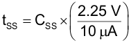
To maintain a controlled power up, the UCC28070A has been designed with an adaptive soft-start function that overrides the internal reference voltage with a controlled voltage ramp during power up. On initial power up, once VVSENSE exceeds the 0.75V enable threshold (VEN), the internal pulldown on the SS pin is released, and the 1.5mA adaptive soft-start current source is activated. This 1.5mA pullup almost immediately pulls the SS pin to 0.75V (VVSENSE) to bypass the initial 25% of dead time during a traditional 0V to VREGULATION SS ramp. Once the SS pin has reached the voltage on VSENSE, the 10μA soft-start current (ISS) takes over. Thus, through the selection of the soft-start capacitor (CSS), the effective soft-start time (tSS) may be easily programmed based on Equation 21.
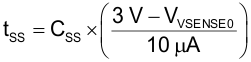
Often, a system restart is desired following a brief shutdown. In such a case, VSENSE may still have substantial voltage if VOUT has not fully discharged or if high line has peak charged COUT. To eliminate the delay caused by charging CSS from 0V up to the precharged VVSENSE with only the 10μA current source and minimize any further output voltage sag, the adaptive soft start uses a 1.5mA current source to rapidly charge CSS to VVSENSE, after which time the 10μA source controls the VSS rise at the desired soft-start ramp rate. In such a case, tSS is estimated as follows:
where
- VVSENSE0 is the voltage at VSENSE at the moment a soft start or restart is initiated
For soft start to be effective and avoid overshoot on VOUT, the SS ramp must be slower than the voltage-loop control response. Choose CSS ≥ CVZ to ensure this.
 Figure 6-4 Soft-Start Ramp Rate